Frequency-Modulated Continuous-Wave Radar
Table of Contents
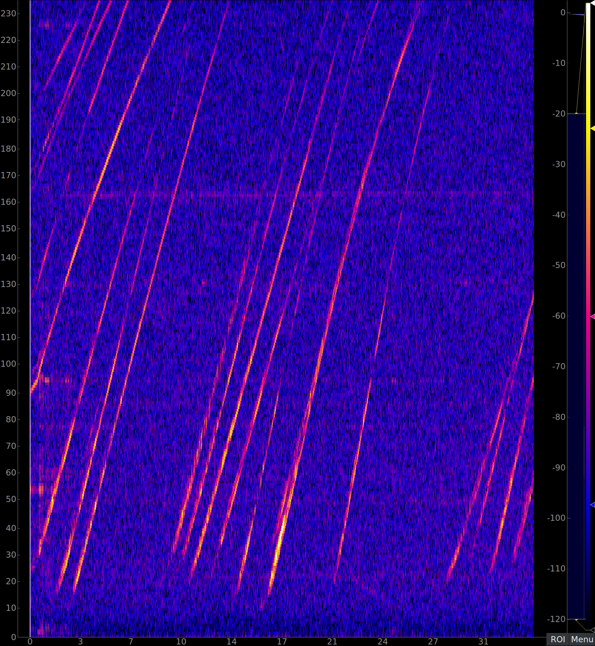
Figure 1: Real-time range detection performed by radar. Distance (y-axis) is in meters and the time (x-axis) is in seconds. Magnitude is in dBFS relative to the max ADC input.
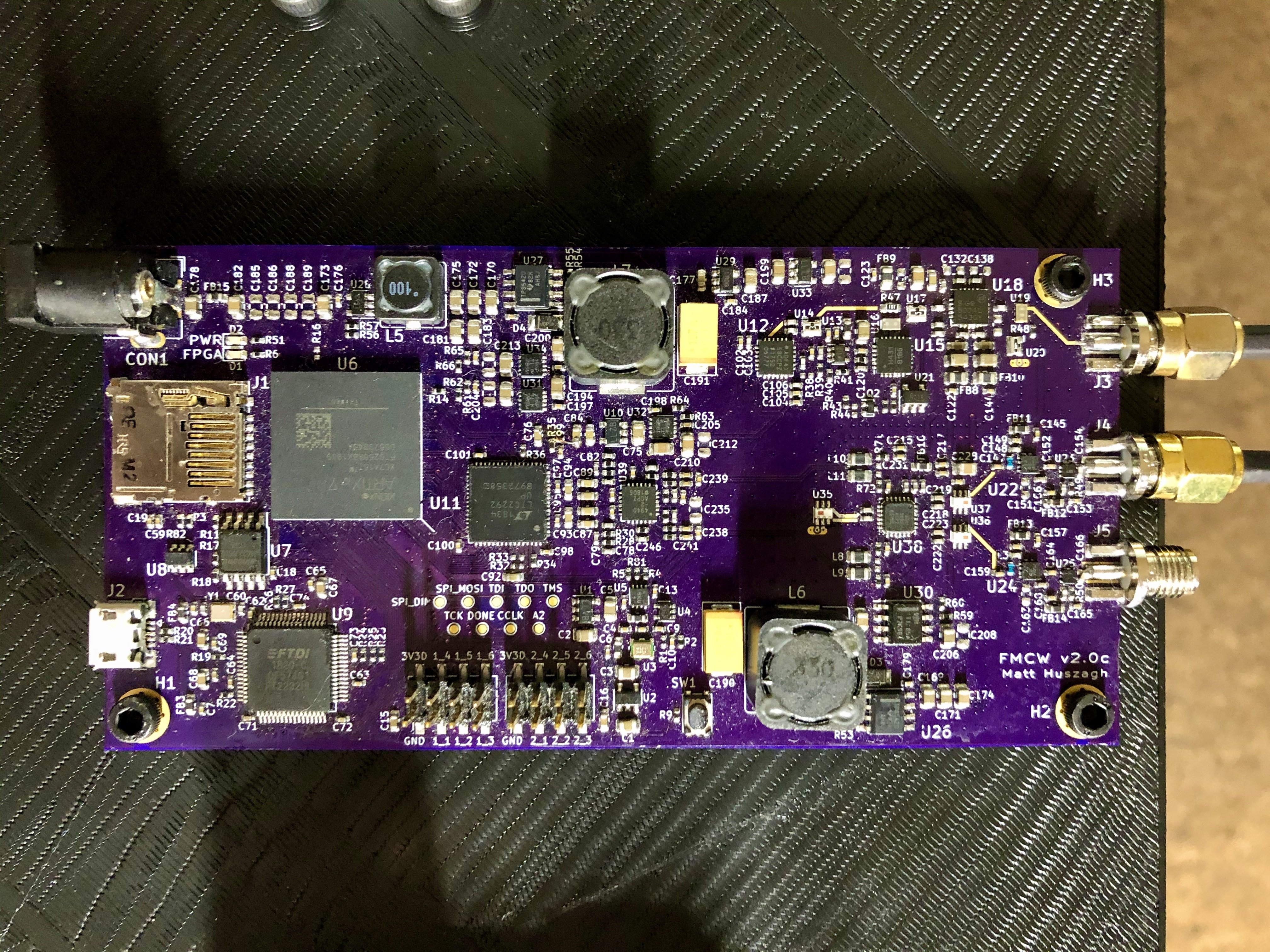
Figure 2: Main radar PCB (rev1).
1. Introduction
This blog presents the key details of an FPGA-based radar I developed and built, including a summary of the relevant physics followed by more in-depth descriptions of the various hardware components and related FPGA and PC (linux) programming. It focuses on design and implementation details rather than how to use this radar. For usage information see the README. My formal education is in physics, not electrical engineering or software programming. But after a few years trading financial derivatives I decided that I wanted to do something more fun and challenging, and I chose this project to develop several areas of technical knowledge — including electrical engineering and FPGA programming — and apply them in a practical way.
I was originally motivated by an excellent design for a radar by Henrik Forsten that provides a valuable description of many key components. My debt to Henrik and appreciation of his work are great. Building on what he did, I created a design that uses an FPGA in a much more significant way — to perform all major real-time processing of the radar reception data — and wrote the interfacing host PC code from scratch. This met my twin goals of being able to configure hardware for large-volume data processing and developing a diverse set of electrical engineering and programming skills.
The biggest and most rewarding challenge in this project involved the FPGA gateware design and programming (described here). Other aspects of the project — characterizing the radar physics, designing and configuring elements of the printed circuit board (PCB) to implement numerous sub-processes and to avoid or eliminate signal problems, simulating and designing the distributed microwave structures, and programming the PC to interface with the FPGA and other hardware elements — were also uniquely valuable. In particular:
- I've completely rewritten the FPGA code so that all the signal processing is now performed in real time on the FPGA. I've done this without changing the actual FPGA device used. I've also added tests and some formal verification to accompany the new code.
- I've written a high-level Python interface to the OpenEMS electromagnetic wave solver and simulated and designed the microwave parts of the radar using this tool. These simulations are described in the RF Simulation section of this post.
- I've rewritten the host PC software from scratch to accommodate the new FPGA code.
- I've redone the PCB layout from scratch in order to modify the design for a deprecated part.
- I designed and 3D printed horn antennas and a mount for the radar.
- I've added a few analog simulations of relevant parts of the PCB using Ngspice.
The full project code is open source and can be viewed on GitHub. I hope you gain some benefit from what follows. Please do not hesitate to contact me if you have any questions.
2. Miscellaneous Notes
Several preliminary comments about this post are in order.
Although I've put a lot of time into this project, it is still a work in progress. In particular, there have been two major iterations of the hardware design, referred to as rev1 and rev2 (both revisions are maintained in the source code repository). All results presented in this post are from rev1 because I have not yet built rev2. However, these results pointed to a few shortcomings that I designed rev2 to fix. Because this post is meant as a description of the right way to do things, it presents the design considerations for rev2. In several instances, however, I have made references to aspects of rev1 in order to explain shortcomings in certain results.
Finally, a number of sections go into a considerable amount of detail. While I believe these sections are very valuable, I don't expect everyone to read them in full, so I've placed a link at the beginning of them to allow the reader to jump to the next high-level section. Still, the detail's there and I encourage you to read it.
3. Overview
At a very high level, a radar (depending on the technology used) can detect the distance to a remote object, the incident angle to that object, the speed of that object, or some combination of these. This radar currently just detects distance. The hardware supports angle detection too (and Henrik's version does this), but at this stage I have not yet written the code for that.1
Figures 3 and 4 show what the radar looks like with the 3D-printed antennas and mount.
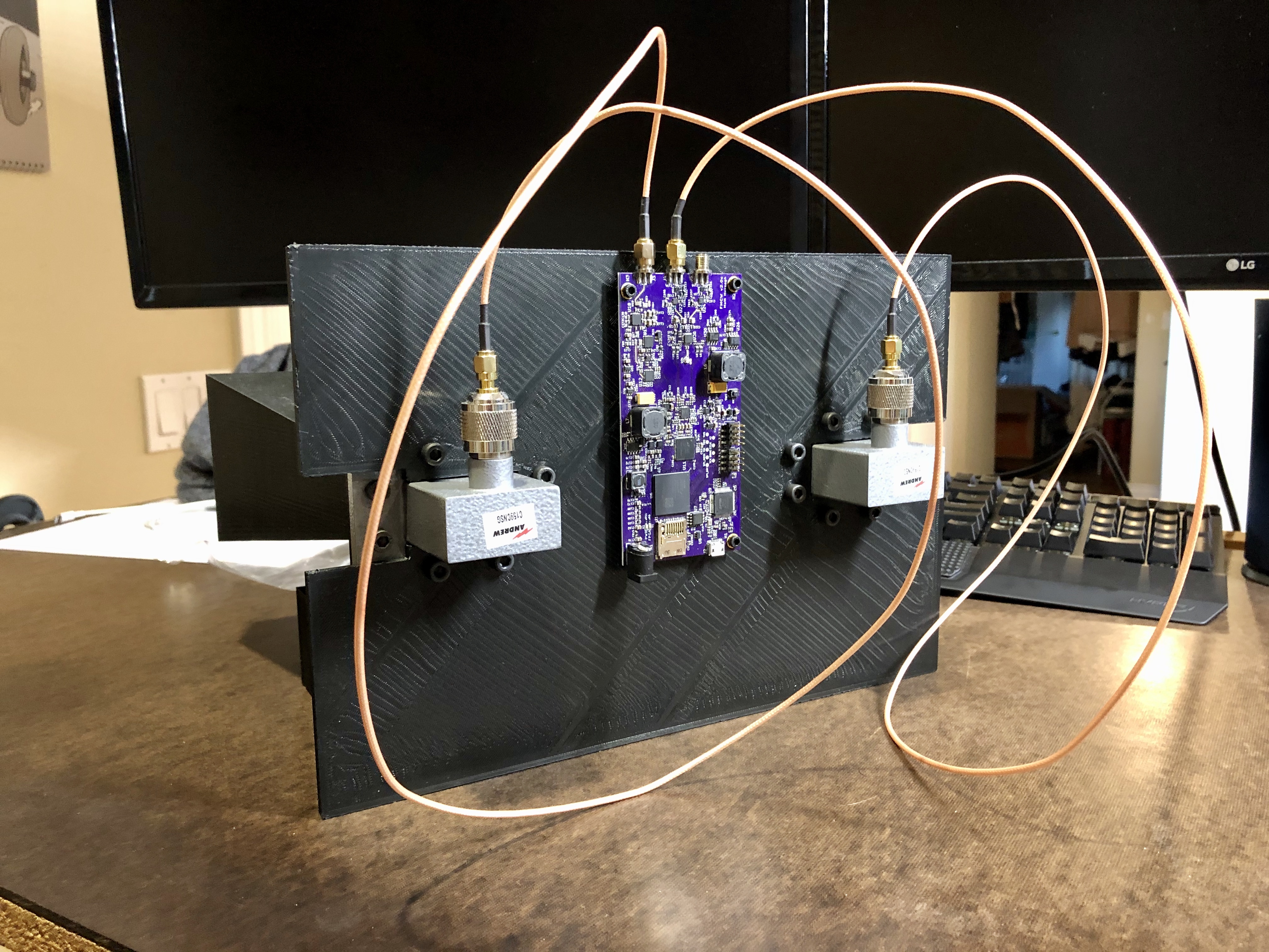
Figure 3: Radar plus mount from back side.
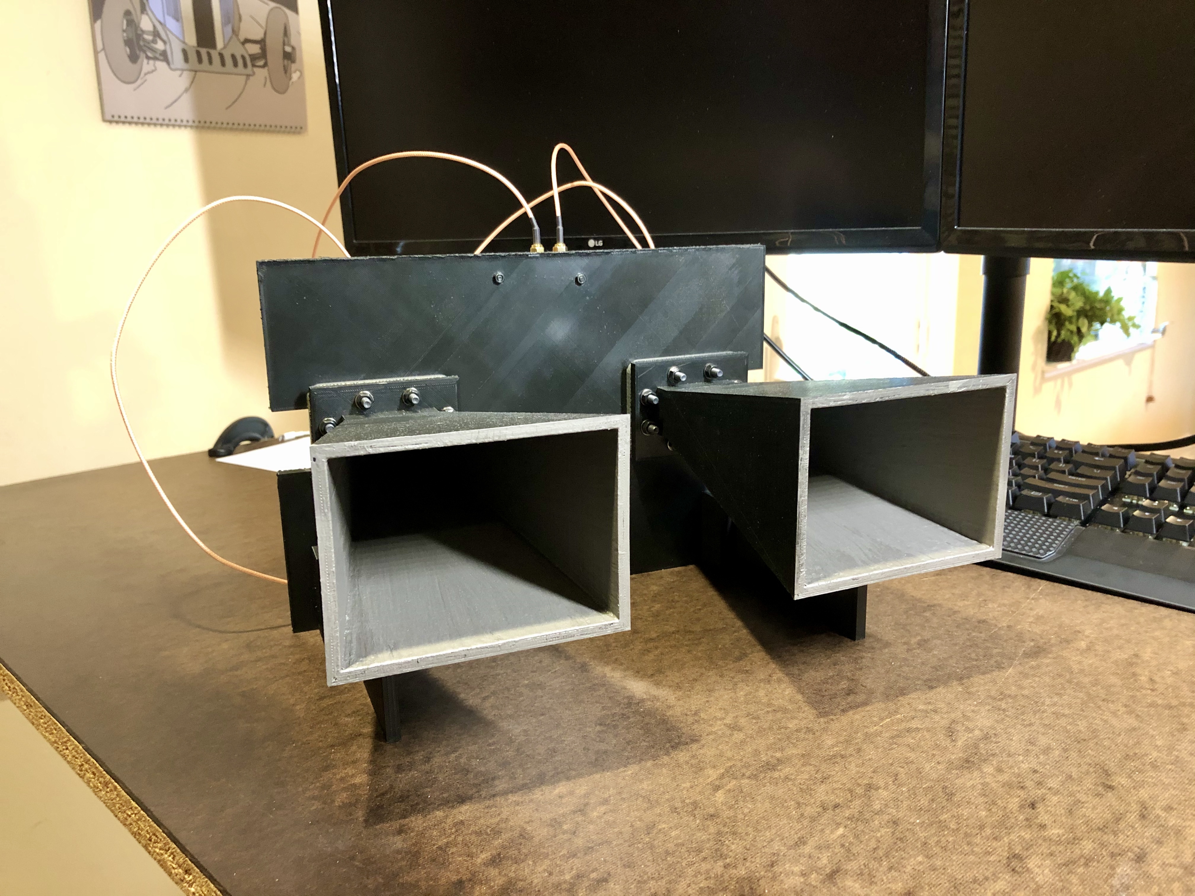
Figure 4: Radar plus mount from front side.
Figure 1 shows the output produced when observing cars on a highway from an overhead bridge.
Broadly, the radar works by emitting a frequency ramp signal that reflects off a remote object and is detected by a receiver. Because the transmitted signal travels through air at the speed of light and its frequency ramps at a known rate, the frequency difference between the transmitted and received signals can be used to determine the distance to the remote object.
4. Physics
4.1. Operating Principle
The distance to a remote object is
| (4.1.1) |
where is the time delay between the transmitted and received signals and is the speed of light in air. The factor of accounts for the fact that the signal must travel the round-trip distance. The transmitted and received signals at the input to the mixer (see the PCB block diagram) are shown in Figure (as pictured, these are sawtooth ramp signals with a time delay between ramps).

Figure 5: Frequency ramp signal as generated by the transmitter and as seen by the receiver.
The ramp slope and duration are explicitly programmed. So, by finding the frequency difference between the transmitted and received signals, we can find the time difference and thus the distance:
| (4.1.2a) | ||||
| (4.1.2b) |
To find the frequency difference we note that the transmitted signal has the following form (I've restricted and to be within the bounds of a single ramp period, which is similarly restricted by the implementation):
| (4.1.3a) | ||||
| (4.1.3b) | ||||
| (4.1.3c) |
where is the transmission signal amplitude.
The received signal is just a time-delayed copy of the transmitted signal with a different amplitude. The amplitude changes because energy is lost as the wave propagates through air and the signal is amplified by the receiver. Energy is proportional to the amplitude squared. The expression for the received signal is
| (4.1.4a) | ||||
| (4.1.4b) | ||||
| (4.1.4c) |
We can also write this expression as
| (4.1.5) |
where . It's easy to see that this is approximately equal to . Look back at Eq. (4.1.1). If we take the max distance to be (see the range section), the maximum time delay is less than . The time delay is usually much less, since we typically restrict ourselves to . In contrast, the value of during a sweep ranges from . So, for almost the entire ramp period, it's fair to assume . Using this approximation, the equation for our received signal turns into
| (4.1.6a) | ||||
| (4.1.6b) |
The product of two sine functions can be equivalently represented as
| (4.1.7) |
In other words, as a combination of a sinusoid of the frequency sum and a sinusoid of the frequency difference. It's precisely the frequency difference that we want. Moreover, the frequency sum will be much higher than the frequency difference (about 4 orders of magnitude in our case). As a result, the circuitry that we use to pick up the difference frequency won't detect the sum frequency. Using this knowledge, we see that if we multiply the transmitted and received signals we get
| (4.1.8a) | ||||
| (4.1.8b) | ||||
| (4.1.8c) |
So, using a Fourier transform on the mixer output will tell us the frequency difference and thus the distance.
4.2. Range
It's possible to relate the range of a remote object to the power received at a reception antenna using something known as the radar range equation. I've derived this equation in the range equation derivation section. The resulting equation is
| (4.2.1) |
All of these variables except reception power are constant and reasonably easy to calculate. They are presented in Table 6.
(See the power amplifier section for how the transmitted power was determined, and the horn antenna section for the antenna gain.)

Figure 6: Values in range equation.
This leaves us with a function relating range to received signal power. For a reason that will be clear momentarily, we've used received signal power as the dependent variable in Figure 7.

Figure 7: Received signal power plotted as a function of remote object distance.
In the maximum and minimum received power sections, we derive the receiver power range as a function of the measured difference frequency. This frequency can be directly related to the distance using Eq. (4.1.2b). Although we can change the ramp duration and frequency bandwidth to our liking, for this calculation I'll use the software defaults of and . I've replotted the range plots from those sections as a function of distance in Figure 8, along with the received signal power we just found. Additionally, I've added to the minimum power. The reason for this is that the signal has to be somewhat stronger than the background noise to be detectable. The choice of is somewhat arbitrary, but is reasonable and frequently used.

Figure 8: Radar visible range. The visible range is bounded by the intersection distances of received power with the minimum and maximum detectable powers.
The visible range corresponds to the range where the actual received power is between the minimum and maximum detectable powers. Additionally, we're restricted to distances corresponding to frequencies less than the Nyquist frequency (, or ). From Figure 8 we see that this corresponds to distances between about and .
It is important to note that this visible range (and the calculations performed in the minimum and maximum received power sections) correspond to just one possible radar configuration. For instance, it is possible to reconfigure the radar to work for longer ranges without making any hardware or FPGA modifications.
From the Operating Principle section (specifically, Eq. (4.1.2b)), we see that we can can perform some combination of decreasing and increasing to increase the range. Let's set and . Figure 9 shows the range in this configuration.

Figure 9: Radar visible range for and .
This plot shows that we should be able to detect remote objects out to . Moreover, we can probably achieve even longer ranges by adjusting and further.
Finally, it's worth mentioning that in the old version of the PCB that I'm currently using for testing, the noise floor is higher than it should be (the new version is designed and should fix this issue, but is not yet ordered and assembled). I'm measuring a noise floor of rather than the theoretically-predicted value of . The difference has the effect of increasing the minimum power line in each of the above plots by that amount. This decreases the maximum range on the old version somewhat.
4.2.1. Range Equation Derivation
Next high-level section: PCB Design
Most of the steps in this derivation are identical to the derivation for the well-known Friis transmission formula.
Start by imagining that our transmission antenna is isotropic. The power density at some remote distance is given by
| (4.2.1.1) |
where is the transmitted power. The comes from the fact that the isotropic antenna by definition radiates power equally in all directions and therefore the power density at some distance is inversely related to the surface area of the sphere centered at the transmission antenna. Now we replace the isotropic antenna with an antenna with gain in the direction of and the equation becomes
| (4.2.1.2) |
At this distance, , the transmitted signal reflects off a remote object. The total reflected power is
| (4.2.1.3a) | ||||
| (4.2.1.3b) |
where is the cross-sectional area of the remote object. This is a bit of a simplification, since the total reflected power will be dependent on several other factors such as the material properties of the remote object and its shape. We lump all these additional factors into the cross-sectional area, which therefore generally is not exactly equal to the object's actual cross-sectional area.
We now imagine the remote object simply as a remote isotropic antenna with transmission power given by the reflected power shown above. And we use the same method as the first step to find the power density available at the reception antenna:
| (4.2.1.4a) | ||||
| (4.2.1.4b) |
To find the actual received power, we multiply the power density by the reception antenna's effective aperture and efficiency:
| (4.2.1.5a) | ||||
| (4.2.1.5b) | ||||
| (4.2.1.5c) |
This is the final result. We could equivalently rearrange our equation in terms of the distance,
| (4.2.1.6) |
In our case the transmission and reception antennas are identical, so the equation simplifies to
| (4.2.1.7) |
5. PCB Design
Figure 10 shows a simplified implementation of how the radar PCB works. The data processing (shown as part of the FPGA section) is more flexible in the actual implementation. Notably, the user can decide what processing to perform and whether this processing should be performed on the FPGA or on the host PC (see the FPGA and software sections for more detail).

Figure 10: FMCW radar block diagram. Note that for efficiency reasons downsampling is actually performed as part of the FIR filter. Functionally, the result is identical.
A frequency synthesizer generates a sinusoidal signal that ramps in frequency from to over a duration of (the ramp start, stop and duration are all user-configurable at runtime in software). The signal is then amplified and most of the power is sent to the transmission antenna. The remaining power is redirected to a mixer for multiplication with the received signal. The echo of the transmitted signal is picked up by a reception antenna and amplified with a low-noise amplifier followed by a high-frequency amplifier. This amplified signal is mixed with the coupled portion of the transmitted signal and output as a differential signal. The mixer output is passed through a lowpass filter, which, together with an intermediate frequency amplifier, passes and amplifies signals between about and . The signal is then digitized at a sampling rate of and passed to the FPGA. The FPGA first uses a polyphase FIR filter to simultaneously filter signals of frequency greater than and downsample the signal by a factor of 20, which reduces the computational load for subsequent processing/transmission stages. The signal is then multiplied by a kaiser window and finally transformed into its frequency composition with a 1024-point fast Fourier transform (FFT). The frequency bins are then sent to a host PC for further processing and real-time plotting.
5.1. Transmitter
The transmitter is responsible for generating a frequency ramp that is transmitted through space by an antenna and coupled back into the receiver. An ADF4158 frequency synthesizer and voltage-controlled oscillator (VCO) together generate the ramp signal. A resistive splitter then divides the signal, sending a quarter of the input power to the power amplifier for transmission and another quarter back to the frequency synthesizer (see the frequency synthesizer section). The power amplifier amplifies the signal, most of which is sent to the antenna for transmission. The remainder is coupled back to the receiver. The transmitter is shown in Figure 11.

Figure 11: Transmitter block diagram. I included a transmission line after the VCO to indicate that a transmission line with characteristic impedance of is required for each connection after the VCO. I omitted most of them in the diagram to save space, but they are present on the physical PCB.
5.1.1. Frequency Synthesizer
Next high-level section: Receiver
The ADF4158 frequency synthesizer is based on a fractional-N phase-locked loop (PLL) design. The device is highly configurable, which can be viewed in the datasheet. Chapter 13 of the Art of Electronics (3d ed.) (AoE) provides an excellent description of how a PLL works. I explain the relevant points here. The frequency synthesizer consists of a phase detector and VCO (our VCO is an external component). Figure 12 shows a block diagram of the synthesizer (note that this diagram has been adapted from AoE).

Figure 12: PLL block diagram. This has been adapted from the Art of Electronics, 3d edition.
The phase detector, as the name suggests, outputs a voltage signal which corresponds to the difference in phase between two input frequencies. The VCO generates a frequency that is proportional to an input voltage. (Disregard the frequency divider blocks for a minute. We'll get back to them.) is a reference frequency. In our case this is a clock frequency. Imagine that the rising edge of occurs before the rising edge of . In response, the phase detector increases it's output voltage corresponding to the duration of time that leads . This causes the VCO output frequency to increase accordingly and causes the next edge of the VCO output to occur sooner than the previous one. So, the phase gap diminishes or reverses. The opposite occurs when lags behind . The phase detector is detecting differences in phase, not frequency. However, any differences in frequency will lead to phase differences, and thus the phase detector will cause the frequency and phase of to converge to that of .
All we've done so far is take and generate another signal with identical frequency and phase, which isn't particularly useful. This is where the frequency dividers come in. The R divider takes and outputs a frequency . The N divider does the same thing for . So, what we're doing is setting
| (5.1.1.1a) | ||||
| (5.1.1.1b) |
By setting much larger than , we can generate an output frequency that is much higher than the reference frequency. Figure 12 isn't completely accurate. What we've shown is an integer-N frequency synthesizer, whereas the device we're using is a fractional-N frequency synthesizer. The practical difference is that our value of can be non-integral, which allows finer-grained control of the output frequency.
5.1.2. Resistive Power Splitter
Next high-level section: Receiver
A resistive splitter is a circuit that splits the power at its input between two outputs. The splitter used in this design splits the power evenly between both outputs, though there are splitters designed for uneven splits. Because the splitter is resistive, it loses half of the input power to heat. This leaves below the input power at each output. A common alternative to a resistive splitter is a Wilkinson power divider. The power divider has the benefit of being lossless. That is, the power at each output will be below the input. However, the price paid for this improved efficiency is bandwidth. The reason for this is that each branch of a Wilkinson divider is set to a quarter wavelength. Because wavelength is inversely related to frequency, this will only be suitable for a limited frequency band. The power divider, by contrast, just requires 3 resistors and so its bandwidth is defined by the parasitic values of these resistors.
Our requirements for the splitter or divider are not very demanding. The bandwidth is limited and the power available to the splitter is enough for each output even with the loss. Also, the power is low enough that the heat dissipation doesn't pose a problem. Therefore, using either of these devices would have worked fine. I've opted to use the splitter since this allows us to use one less attenuator and therefore costs marginally less.
5.1.3. Attenuator
Next high-level section: Receiver
An attenuator is a relatively simple circuit that produces an output power which is a desired fraction of the input power. Although I've used an IC for tighter tolerance and better frequency characteristics, the equivalent schematic is very simple and shown in Figure 13. There are several different resistor configurations to create an attenuator. The Pi attenuator shown below is just one of them.

Figure 13: Pi attenuator schematic.
We can get an even more complete picture if we explicitly show the source and load resistance. This is shown in Figure 14.

Figure 14: Pi attenuator schematic with source and load resistance included.
Typically, our source and load impedance will be matched to the characteristic impedance: . Now we need to choose and for the desired attenuation, but subject to the constraint that the attenuator does not present an impedance mismatch and cause signal reflections. To satisfy this, we constrain the Thévenin network of resistors to the right of to be equal to the characteristic impedance, . It is then a simple matter of algebra to show that this sets the relation between , and to be
| (5.1.3.1) |
To find the attenuation, we need to find the voltage transfer function for the attenuator, . The attenuation will be the decibel value of the inverse of this ratio:
| (5.1.3.2a) | ||||
| (5.1.3.2b) | ||||
| (5.1.3.2c) | ||||
| (5.1.3.2d) | ||||
| (5.1.3.2e) |
Finally, we can rearrange our equations to represent the attenuator resistors in terms of the voltage transfer function, , and decibel attenuation, , which are more useful:
| (5.1.3.3a) | ||||
| (5.1.3.3b) | ||||
| (5.1.3.3c) | ||||
| (5.1.3.3d) |
5.1.4. Directional Coupler
Next high-level section: Receiver
A coupler is a device that is able to share the power of a signal at an input port between two output ports. Its schematic depiction is shown in Figure 15.

Figure 15: Directional coupler schematic.
The signal enters at the input port and most of the energy passes through to the transmitted port. Some input energy, however, exits through the coupled port where the amount is given by the coupling factor. See the relevent RF simulation section for more information on how this works. The insertion loss describes how much of the input power makes it to the transmitted port.
The equations for coupling factor and insertion loss are
| (5.1.4.1a) | ||||
| (5.1.4.1b) |
The coupler we use has a coupling factor of and the power amplifier has an output power of which gives a coupled power of . The coupler's insertion loss is , which means the transmitted power is nearly the same as the input power, and so we'll take it to be .
Another important quantity for a coupler (it is often one of the most important criteria for assessing the quality of a coupler) is the coupler's directivity. It is given mathematically as
| (5.1.4.2) |
The directivity represents the ratio of the power available at the isolated port to the power available at the coupled port. Ideally, no power makes it to the isolated port, which would make the directivity infinite. Directivity permits the coupler to differentiate between forward and reverse signals. Having a high directivity is crucial for many devices (e.g. VNAs) but is less critical in our application. Indeed, the directional coupler used here was designed for simplicity of fabrication and to consume minimal board area, but exhibits poor directivity.
5.1.5. Power Amplifier
Next high-level section: Receiver
The power amplifier does exactly what its name suggests: it increases the signal power for transmission. This design uses a SE5004L power amplifier. The most important metrics for us to consider when choosing a power amplifier are the gain and compression point. We also, of course, need to ensure the operating frequency range accommodates our signal frequency. This power amplifier has a small signal gain of and an output compression point of . Its input power is , which puts the output power at , well below the compression point. We could increase the max range somewhat by increasing the power amplification (see the range section). However, this would also increase the minimum range, which isn't a great tradeoff. Moreover, increasing the power amplification would increase the power consumption of the board and heat dissipation, which we would need to mitigate. Finally, there are easier ways of increasing the max range, for instance by changing the intermediate frequency (IF) amplifier frequency response.
5.2. Receiver
A block diagram of the receiver is shown in 16. Its function is to capture the transmitted signal echo, amplify it without introducing too much noise, mix it with the transmitted signal down to an intermediate frequency, filter out non-signal frequencies and then amplify it again for digitization by the analog-to-digital converter (ADC). A simplified block diagram of the receiver hardware is shown below. Note that this is just one of two identical receivers. The mixer and differential amplifier support two separate differential signal pairs, so that circuitry is shared between both receivers.

Figure 16: Receiver block diagram.
5.2.1. Dynamic Range
The radar's dynamic range is the ratio between the maximum signal the receiver can process and its noise floor. See those sections to see how the dynamic range was computed. We find that the theoretical dynamic range is equal to about and roughly constant across the signal bandwidth of interest. This is shown in Figure 17.

Figure 17: Dynamic range as a function of frequency.
As discussed in the range section, the actual noise floor is higher than the theoretical value. A plot of the noise floor up to the decimated Nyquist frequency is shown in Figure 18.
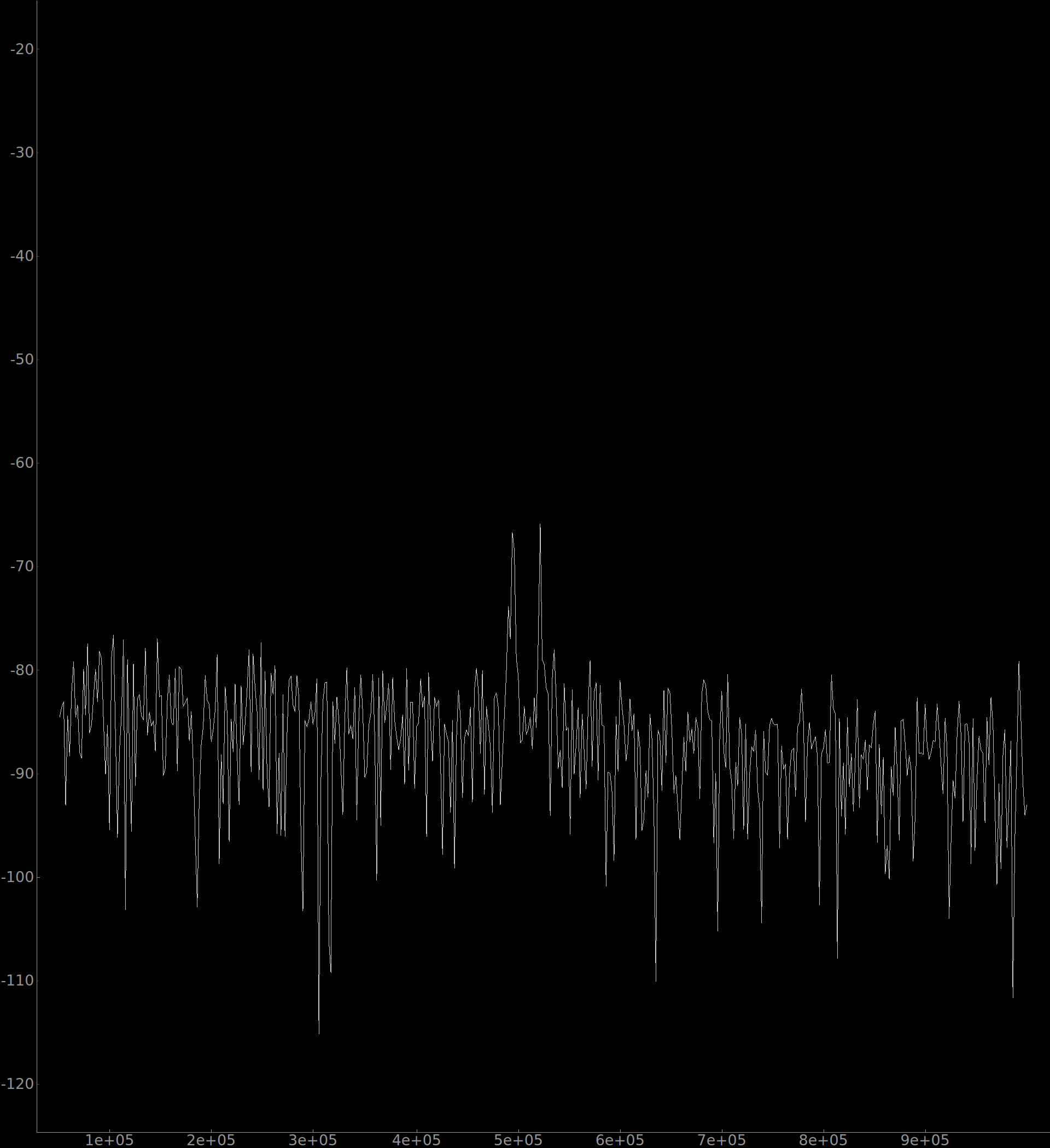
Figure 18: Revision 1 PCB noise floor ( to ). Average value is approximately , compared with the theoretical value of . The two spikes in the middle of the plot are caused by a noisy voltage converter switching at . The noise floor should be significantly improved in the revision 2 PCB.
5.2.1.1. Maximum Power
To find the maximum detectable power that avoids distortion, we can work backward from the ADC input voltage range of . The IF amplifier amplifies this signal with a frequency-dependent gain. Therefore, the maximum power will also depend on frequency. The full sine wave ADC input and IF amplifier gain together give us the maximum mixer voltage output, which we can convert to a power level by first converting it to a root-mean-square (RMS) voltage value and then to an average power level using the mixer differential output resistance of . The equation for this is
| (5.2.1.1.1a) | ||||
| (5.2.1.1.1b) |
where is the voltage amplitude. Every component between the mixer input and the receiver antenna is matched to , so we can convert our mixer output power to a value and subtract the gain of the mixer, radio frequency (RF) amplifier and low-noise amplifier (LNA) to arrive at the maximum antenna power. The collective gain of the LNA, RF amplifier and mixer (see minimum power section) is . I've performed this calculation over the full range of the IF amplifier gain. The results are plotted in 19.

Figure 19: Maximum received power as a function of frequency.
5.2.1.2. Minimum Power
Computing the minimum detectable power is more complicated than computing the maximum power. It requires first finding the voltage noise at the ADC input and then using the same procedure as in the maximum power section to relate this to an equivalent input power level.
We start by computing the thermal noise power at the reception antenna. This can be found with the equation
| (5.2.1.2.1) |
where is the Boltzmann constant, is room temperature and is the bandwidth. I'll start by using the Nyquist frequency for the bandwidth, , though this will decrease when we incorporate the process gain of the FFT. This evaluates to
| (5.2.1.2.2a) | ||||
| (5.2.1.2.2b) |
The LNA and RF amplifier have their inputs and outputs matched to , and the mixer has its input matched to . As a result, we can simply add the collective noise figure of these components to find the noise power at the mixer output. The equivalent noise figure of multiple impedance-matched components chained together can be computed using the Friis formula for noise:
| (5.2.1.2.3) |
where denotes a noise factor (noise figure is the decibel value of noise factor) and denotes the non-dB gain. The subscripts refer to the stage. The result is presented in Table 20.

Figure 20: Noise figure and gain of each receiver stage, along with the cumulative values.
So, adding to the antenna noise power leaves us with noise power at the mixer output. As in the maximum power section, we need to convert this to a voltage noise level since our components no longer have matched impedance values. The rest of the components use impedance bridging, so there is negligible voltage loading between stages. This voltage noise level will be multiplied by the IF amplifier gain and then added to its noise contribution, which we found to be in the IF amplifier noise section ( over the full bandwidth). Finally, we add the found to be the ADC noise contribution and the quantization noise. The quantization noise power is assumed to be spectrally flat over the full Nyquist bandwidth and equal to
| (5.2.1.2.4) |
where is the LSB voltage. Next, we have to adjust this value for the processing gain we get by filtering, downsampling and performing an FFT on the data. The easiest method to compute this is by noticing that we computed the voltage noise for the full Nyquist rate, but our FFT bin bandwidth is . So, the voltage noise we see after processing is the old voltage noise divided by the square root of the ratio of these bandwidths. Then, we can convert this back to an input power level using the same procedure we used before. The result is plotted in Figure 21.

Figure 21: Minimum received power as a function of frequency.
5.2.2. Mixer
Next high-level section: Differential Amplifier
A multiplicative mixer is a device that multiplies two input signals. Many mixers (including the one used in this design) are based on a Gilbert cell, whose schematic is shown in Figure 22.

Figure 22: Gilbert cell schematic.
The lower differential pair sets the gain of each of the top two differential pairs. For instance, if is made positive there will be more total emitter current for the left differential pair than for the right differential pair. The top input, , is cross connected between the top transistors. That is, is connected to the base of two transistors whose collectors are tied to different polarities of .
To understand the operation, start by setting . It doesn't matter what we set to, will always be 0. For instance, if , 's collector current will be greater than that of , but 's collector current will exceed that of by the exact same amount (remember so the differential gain of each amplifier is identical). Since the voltage drop across the leftmost is determined by the combined currents to 's and 's collectors and the drop across the rightmost is determined by the combined currents to 's and 's collectors, the voltage drops will be identical. When the collector current for each transistor within a differential pair will be the same. So, even if we change to change the total emitter current for each upper differential pair, the output voltage will still be 0.
If we set , this increases the total emitter current for the left differential pair compared to the right differential pair. Then, will increase 's and 's collector currents and decrease those for and , but it will change 's and 's collector currents more than it changes the collector currents for and . So the net effect is that . We can continue to analyze the circuit using the same procedure to find that the circuit's voltage transfer function is given by
| (5.2.2.1) |
where is some gain factor.
5.2.3. Differential Amplifier
The differential amplifier's input circuitry is worth discussing because it affects the amplifier's frequency response. There are three logical parts to this, separated by dashed lines in Figure 23. The pullup resistors at the mixer output set the DC bias point of the output to . This is followed by an LC lowpass filter. And then the differential amplifier acts as a second-order active bandpass filter, with roughly of gain (though it varies with frequency). The DC blocking capacitors in the active filter serve an additional purpose, which is to allow the differential amplifier's input voltages to float down to the acceptable input range. This is critical because the bias point would be too high for the amplifier, which has a supply voltage of .

Figure 23: Differential amplifier, including input filter.
The frequency response of this circuit is shown in Figure 24.

Figure 24: IF amplifier voltage gain and phase response from DC to (left) and limited to the signal frequency range (right).
5.2.3.1. Noise
Next high-level section: Digitization, Data Processing and USB Interface
The ADA4940 differential amplifier datasheet provides a method for estimating the output noise voltage given the feedback circuitry. Unlike the other receiver components, the differential amplifier is a relatively low-frequency component and does not have its ports matched to . As a result, we characterize its noise in units of , instead of as a noise figure.
To calculate the root-mean-square (RMS) output differential voltage noise density, the datasheet provides the equation
| (5.2.3.1.1) |
where denotes 8 different output noise sources. These sources can be calculated using the equations below. I've simplified them based on the fact that our resistors are the same at each input of the amplifier. The equations for the individual noise sources are
| (5.2.3.1.2a) | ||||
| (5.2.3.1.2b) | ||||
| (5.2.3.1.2c) | ||||
| (5.2.3.1.2d) | ||||
| (5.2.3.1.2e) | ||||
| (5.2.3.1.2f) | ||||
| (5.2.3.1.2g) | ||||
| (5.2.3.1.2h) | ||||
| (5.2.3.1.2i) | ||||
| (5.2.3.1.2j) | ||||
| (5.2.3.1.2k) | ||||
| (5.2.3.1.2l) | ||||
| (5.2.3.1.2m) | ||||
| (5.2.3.1.2n) | ||||
| (5.2.3.1.2o) | ||||
| (5.2.3.1.2p) | ||||
| (5.2.3.1.2q) |
Plugging all this in, we get .
5.3. Digitization, Data Processing and USB Interface
An ADC converts differential analog signals from the receiver into 12-bit digital signals that are then sent to the FPGA for processing. The FPGA supports a two-way communication interface with the FT2232H USB interface chip that allows it to send processed data to the host PC for further processing and receive directions and a bitstream from the PC. A block diagram of this is shown in Figure 25. I've omitted the ADC's second input channel since it's identical to the first. Both channels are time-multiplexed across the same 12-bit data bus to the FPGA.

Figure 25: Digitization and data processing block diagram.
5.3.1. ADC
This design uses an LTC2292 ADC.
5.3.1.1. Input Filter
The ADC employs common-mode and differential-mode lowpass filters at its analog inputs (see Figure 25). The series resistors and outer capacitors serve as a lowpass filter for common-mode signals with a cutoff frequency of (). The combination of series resistors and the inner capacitor serve as a differential-mode lowpass filter with a cutoff frequency of (). As described in the datasheet, the filters prevent the sample-and-hold charging glitches of the ADC from affecting the IF amplifier (remember the IF amplifier outputs are used for feedback). Additionally, they limit wideband noise, which could alias into our signal. It's also important to keep the resistor values low to limit thermal noise.
5.3.1.2. Noise
The signal-to-noise ratio (SNR) of an ADC is equal to the ratio of the RMS value of a full-wave sinusoidal input (amplitude equal to the maximum input of the ADC) to the voltage noise RMS value. Mathematically,
| (5.3.1.2.1) |
The datasheet reports an SNR of . We can use this to compute the voltage noise over the bandwidth:
| (5.3.1.2.2a) | ||||
| (5.3.1.2.2b) |
5.3.2. FPGA
The heart of this project is its use of an FPGA, which offers unique performance attributes and design challenges. The FPGA serves two purposes: it performs data processing, and it acts as an interface to configure other ICs on the PCB. An FPGA can implement any digital logic circuit, within resource limitations, which gives us a tremendous amount of flexibility in regard to how we process the raw data and how to interact with and configure the other PCB ICs. The benefit of using the FPGA rather than software on the host PC for data processing is that it can run these algorithms faster than traditional software, and it also allows us to ease the burden on the USB data link between the radar and host PC. In regard to the second point, the bandwidth between the radar and host PC is limited by the USB 2.0 High Speed data transfer speeds of , which is an upper bound (the practical speed is lower, typically about ). By using the memory facilities of the FPGA as a buffer, we can send the raw data directly to the host PC and process and plot it in real time. However, if our data link was slower (e.g., our host computer only supported a USB 1.0 interface), we could ease the burden on the data link by performing the processing directly on the FPGA. This works because the FIR decimation filter only keeps 1 sample out of every 20 inputs.
This design uses an XC7A15T FPGA from Xilinx, which is a low-cost FPGA but is nonetheless sufficient for our needs. One additional benefit of using this FPGA is that it is pin-compatible with a number of higher resource count variants. Consequently, if our data processing needs expand in the future, we can use one of those variants as a drop-in replacement without otherwise altering the PCB.
5.3.2.1. Implementation
Next high-level section: FT2232H
The basic building block of an FPGA is a lookup table (LUT). Although LUTs can use any number of bits stored as a power of 2, these higher-level LUTs are all composed of a collection of simple 2-bit LUTs, shown in Figure 26.

Figure 26: 2-bit LUT.
The operation is very simple: to output the bit in the upper register we deassert the select line and to output the bit in the lower register we assert the select line. The register bits, called the bitmask, can be independently set.
We can already use this simple LUT to mimic the behavior of single-input logic gates. If we wanted the behavior of a buffer, we could write a 0 to bit 0 and a 1 to bit 1. The select line acts as the buffer input. A 0 here outputs a 0 and a 1 outputs a 1. To implement a NOT gate, we'd write a 1 to bit 0 and a 0 to bit 1.
It's instructive to double the size of the LUT to see how we can replicate two-input logic gates. A schematic for this is shown in Figure 27.

Figure 27: 4-bit LUT.
The select lines of the leftmost multiplexors are tied together to s0. The truth table for an AND gate is shown in Table 28. I've additionally included the bitmask number to show how the AND gate can be implemented.

Figure 28: Truth table for an AND gate, along with the necessary bit setting for an equivalent LUT.
So, the bitmask necessary to implement an AND gate is the bit in the out column for each bit number. In other words, bits 0 to 2 should be set to 0 and bit 3 should be set to 1. We can adjust this truth table for any other 2-input gate to show the correct bit mask to implement that gate.
Theoretically, we could now implement any combinational digital logic circuit with a sufficiently large interconnected array of these size-4 LUTs. Unfortunately, our processing circuit would be glacially slow. In particular, we haven't added any register elements (apart from the bit mask) so we wouldn't be able to pipeline our processing stream. Actual FPGAs incorporate LUTs and registers into larger structures often called logic blocks, which are designed to optimize pipeline performance for typical use cases.
FPGA implementations also need to address a number of other practical design challenges. Some of the most prominent of these are data storage, multiplication and clock generation and distribution. Although we can store processing data in the registers within logic blocks, we frequently need more storage than this provides. Additionally, using these registers for storage limits their use in pipelining, making the FPGA configuration slower and more difficult to route. To address this need, all but the simplest FPGAs come with dedicated RAM blocks.
Similarly, while LUTs can perform multiplication, they are needlessly inefficient in this regard. Since multiplication is highly critical in digital signal processing (DSP) applications, which is one of the major use cases for FPGAs, FPGAs have built-in hardware multipliers.
Finally, in regard to clocks, FPGAs often need to create derivative clock signals. This allows a portion of a design to be clocked at a much higher rate which correspondingly increases the throughput of the data processing stream. So, they are equipped with a number of phase-locked loops (PLLs). Additionally, it is critical that clock signals reach all registers with as little skew as possible. This makes timing closure (ensuring that all signals reach their destination register at the right time) much easier to achieve by the software tools that allocate FPGA resources. Because of this, FPGAs are built with dedicated, low-skew clock lines to all registers.
FPGAs are highly-complicated devices that require many sophisticated design considerations. This section mentioned only a few of the main ones.
5.3.3. FT2232H
The FT2232H is a USB interface chip that permits 2-way communication with the FPGA and enables us to load a bitstream onto the FPGA. The attached EEPROM chip is required to use the FT2232H in its FT245 synchronous FIFO mode, which allows the full data transfer speed.
5.4. Power
The radar receives of power provided by a barrel jack connector. The power circuitry then converts/regulates this down to the supply voltage expected by each integrated circuit on the PCB. Although the power circuitry is fairly self-explanatory, a few things deserve mention. Buck converters are used to bring the input down to an intermediate voltage level, and then linear regulators take that intermediate voltage and produce the final supply voltage for each component. Buck converters are more energy-efficient than linear regulators, and linear regulators are less noisy than buck converters. By chaining both together, we can get the best of both worlds. In order to achieve the energy efficiency, the buck converters should output a voltage that is only slightly above the target output voltage of the downstream linear regulator. For this to work, the minimum voltage dropout must be below the actual voltage dropout. We can use low-dropout (LDO) regulators to accomplish this.
Additionally, we have to pay special attention to the power supply rejection ratio (PSRR) of the linear regulators. Voltage regulators have high PSRR at low frequencies, but the PSRR typically falls off significantly as the frequency increases. Most of the buck converter noise occurs at its switching frequency, with additional noise at harmonics of this switching frequency (e.g. ). So, we need to ensure that the linear regulator PSRR is sufficiently high at the switching frequency and preferably for the first harmonics as well.
Finally, of course, we need to make sure that the buck converters and linear regulators can supply enough output current for all downstream devices under full load.
5.4.1. Voltage Regulator Implementation
Next high-level section: FPGA Gateware
A simple implementation of a voltage regulator is shown in Figure 29. This has been adapted from AoE.

Figure 29: Simple, non-optimal implementation of a voltage regulator circuit.
The operation of this circuit is very simple. The non-inverting input of the opamp is set by a current source supplying a zener diode. The current source provides a constant current over changes in the input voltage, so the voltage across the zener remains fixed at the desired reference. The inverting input is tied to a voltage divider output from the output voltage. The resistors are chosen to provide a desired output voltage for the reference voltage. Mathematically,
| (5.4.1.1) |
Finally, a darlington pair provides current amplification. So, for instance, even if our opamp could supply only about of current, darlington pairs often have current amplification on the order of or more, so this regulator would be able to supply of current to a downstream device.
It's important to consider 's power dissipation. Specifically, it will dissipate
| (5.4.1.2) |
For large voltage drops and large currents, this can amount to a significant amount of power, which the transistor must be designed to handle. Moreover, this is wasted power, which is the reason for the use of LDO regulators in the radar.
It's also worth noting that this implementation has some drawbacks. For instance, it provides no current limiting and thus could be damaged if the output were shorted.
5.4.2. Voltage Converter Implementation
Next high-level section: FPGA Gateware
The operation of a voltage converter is more complicated than that of a voltage regulator. In this discussion we'll restrict ourselves to buck converters since that is what is used in the radar. That is, converters for which the output voltage is lower than the input voltage. However, the operation of boost converters and inverters is similar.
Figure 30 shows a possible implementation of a buck converter. This schematic has been adapted from AoE.

Figure 30: Simple implementation of a buck converter.
Ignore everything attached to the nMOS gate for the moment. We'll come back to it later. The salient point for now is that the transistor will be switched in a periodic way, with a percentage of that switching, , (called the duty cycle) in the on state and the remaining percentage, , in the off state.
We can describe this circuit with two different equations: one when the transistor is switched on and one when it is off.
In the on state,
| (5.4.2.1a) | ||||
| (5.4.2.1b) | ||||
| (5.4.2.1c) | ||||
| (5.4.2.1d) |
And in the off state,
| (5.4.2.2a) | ||||
| (5.4.2.2b) | ||||
| (5.4.2.2c) | ||||
| (5.4.2.2d) | ||||
| (5.4.2.2e) |
To simplify the analysis, Eq. (5.4.2.2b) approximates as having 0 voltage drop. This is a reasonable approximation since the voltage drop across Schottky diodes is fairly small. If we were designing an actual switching converter we'd have to include this.
We can now impose the constraint
| (5.4.2.3) |
since otherwise the current would increase or decrease without bound. When we substitute in the current changes during the on and off states, we are left with following expression relating the input and output voltages:
| (5.4.2.4) |
Additionally, there are no lossy components here (aside from the small voltage drop between the nMOS drain and source) and so this device is theoretically 100% efficient. That is, . The output capacitor will smooth the output , ramp, and the average output voltage will be given by Eq. (5.4.2.4). Of course, real switching converters exhibit some loss, but the efficiency can often be upwards of 90%.
Before discussing the circuitry driving the transistor gate, it's worth addressing the Schottky diode which appears to play no role in the converter's function. Let's imagine what would happen if the diode were not present. When the transistor switches off, the inductor will go from seeing some current through it (call it ) to almost immediately seeing no current through it. The defining equation of an inductor is , so for very small the inductor creates an enormous spike in the voltage across its leads trying to keep its current constant. This translates into the same huge spike at the nMOS source which is likely to damage the transistor. The presence of the Schottky provides a path for current to flow so that the voltage across the inductor peaks at one Schottky forward voltage drop.
Now we can move on to the gate driver circuitry. The oscillator block produces two signals: a clock pulse and a sawtooth ramp with the same period and phase as the clock pulse. This is shown graphically in Figure 31.

Figure 31: Switching converter duty cycle control. Clock pulse (top) and sawtooth ramp (bottom).
The error amplifier outputs a voltage proportional to the difference between the reference voltage and the divided output voltage. The flip flop in this circuit is a set-reset (SR) flip flop. So, the instant a high voltage arrives at its set input the output will go high, and the instant a high voltage arrives at its reset input the output will go low. The output voltage will remain as the last value it was set as until another high set or reset changes its output. For example, even though the clock pulse drops low immediately after being asserted, the output remains high until the reset pin is asserted. So, when the clock pulse arrives, the output will go high and remain that way until the sawtooth ramps to a voltage higher than the error voltage.
To understand this better imagine what happens when the output voltage is higher than its target set by the feedback loop. In this case, the error amplifier decreases its voltage and the duty cycle of the nMOS is reduced. We determined above that , so this has the effect of decreasing the output voltage. The opposite phenomenon occurs when the output voltage is below its target.
5.5. PCB layout
An image of the complete PCB layout is shown in Figure 32, with images of each layer shown in Figures 32, 33, 34, and 35.
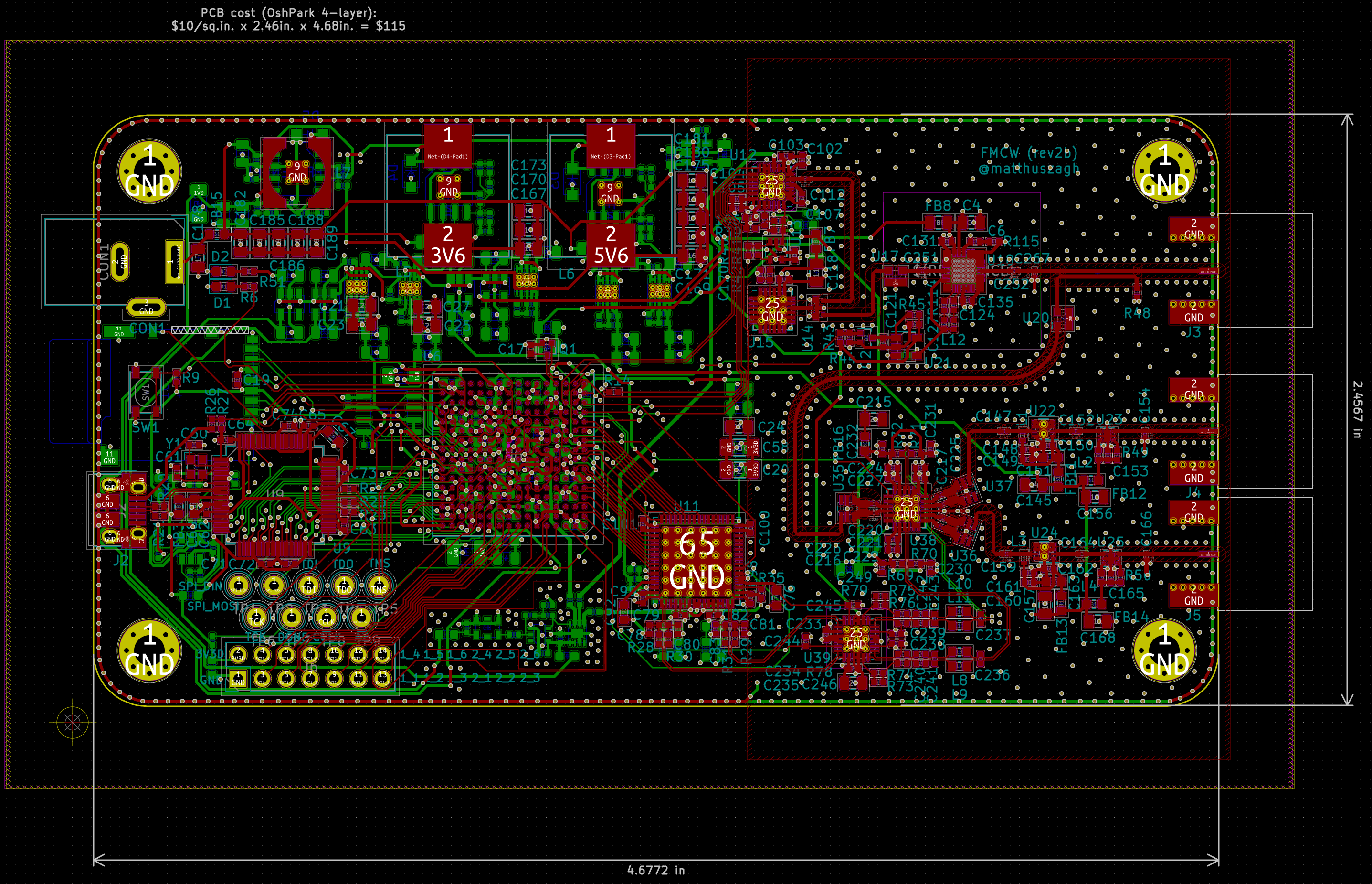

Figure 32: PCB layer 1. The top layer is a signal layer containing the sensitive RF circuitry on the right side and the digital circuitry on the left side.

Figure 33: PCB layer 2. This copper layer is an unbroken ground plane.

Figure 34: PCB layer 3. This copper layer is an almost completely unbroken ground plane.

Figure 35: PCB layer 4. The bottom layer is a signal layer and contains most of the power supply circuitry.
This is a 4-layer PCB in which the top and bottom layers are signal layers and the middle two layers are unbroken ground planes. The right portion of the top layer contains the transmitter and receiver, the left portion of the top layer contains mostly digital circuitry, and the bottom layer is primarily devoted to the power supply circuitry.
This separation of noise-sensitive RF circuitry from the digital circuitry is deliberate. Digital ICs tend to be noisy, and without proper separation, fast digital signals can inject noise into the receiver.
Despite physically separating the digital and analog circuitry, I've decided to use the same unbroken ground plane for each. The rationale for this is that the physical separation should be sufficient to prevent crosstalk from reaching the analog circuits. Moreover, separating the ground planes can create major issues if certain mistakes are made. In particular, there are a few digital signals that pass from the digital section into the analog section. Like all signal traces, these need low-inductance current return paths. When the ground planes are unbroken, the current can return on the ground plane directly adjacent to the relevent signal layer. When the ground planes are broken, the return current needs to find some other path to reach the source. This problem can be avoided by connecting the ground planes with a trace where the signal trace crosses the gap between the ground planes. When this return path is omitted, the fallback return path may have high inductance, creating voltage ringing and noise in the circuit. The additional isolation provided by separated ground planes is typically insignificant and therefore it's safer to keep the ground planes connected.
Another noteworthy decision is that I've used a ground plane on each internal layer, rather than a ground plane on one layer and a power plane on the other layer. Having a dedicated power plane can be useful when most of the PCB's circuitry is served by a single power plane. When this is the case, integrated circuits can receive power through a via between the power rail pin and power plane. This frees up routing space for signal traces. However, this radar requires a substantial number of power rails, which would either require a segmented power plane or a single continuous power plane that only supplies a few power pins leaving the remaining power pins to be supplied by traces. The first solution creates potential hazards when signal traces pass over gaps between individual power planes. The problem with this is identical to the problem raised by breaking up ground planes. Specifically, it can interrupt return currents and add noise to the PCB. The second solution provides us with essentially no benefit. Therefore, it makes more sense to just use an additional ground plane.
The third major decision I've made in regard to grounding is to use a ground fill (a ground plane filling the remaining space on a signal layer) around the sensitive RF circuitry, but not around the digital section on the left side of the top layer or around the power supply on the bottom layer. A ground fill, when used correctly with via fences and via stitching, can increase isolation between sensitive RF traces. A via fence is a series of tightly-spaced ground vias placed on either side of a trace, typically a transmission line. They act as a wall to fringing fields spreading from the transmission line and interfering with other traces or components. These are readily apparent around the microstrip transmission lines in Figure 32.
I've also added stitching vias in this section. Stitching vias are ground vias placed in a regular grid pattern to connect two or more ground regions. They provide a solid electrical (and thermal) connection between the ground fill and inner ground planes. These ensure that regions of the ground fill do not act like unintentional antennas. The general rule-of-thumb for via fences and stitching vias is to place them at a separation of or , where is the wavelength corresponding to the highest frequency signal on the PCB, which in our case is .
I've omitted the ground fill in other regions because of this unintended antenna effect. The improved isolation between traces is important in the sensitive RF section, but is less critical in the digital and power supply regions. Moreover, these regions have a higher density of traces, which would cause a ground fill here to be broken up more. This increases the chance of leaving an unconnected island of copper that could act as an antenna and increase noise in the resulting circuit.
Decoupling (or bypass) capacitor placement is another important consideration for reducing circuit noise. Decoupling capacitors are typically placed adjacent to IC's on a PCB. They serve essentially 2 purposes, which are thematically different but physically the same. The first purpose is that they provide a low-impedance supply of charge to the integrated circuit. This is especially important with digital ICs which draw most of their current during a periodic and small fraction of their clock duty cycle. These are called current transients and the decoupling capacitor acts as the supply of charge for these sudden rises in current draw. Power supplies are unable to satisfy these sudden current demands since they take time to adjust to their current output.
The 2nd reason (which is actually equivalent) is that they prevent noise from leaving the IC and reentering the power supply. The noise is caused by these sudden changes in current. The decoupling capacitors provide a low impedance path for this noise to ground. Analog circuits also require decoupling capacitors, primarily to further isolate themselves from the noise of digital circuits.
Decoupling capacitors can be delineated into 2 size gradations. The first and most important variety are the small (size and value) decoupling capacitors placed immediately adjacent to the ICs whose power supply they decouple. Since these capacitors come in small packages they have low inductance values (inductance is the most critical impedance factor at high frequencies) and therefore are able to provide the current needs for very fast transients. The fact that they are relatively low in value is due to the fact that it's more expensive to put a large capacitance value in a small package. Otherwise, you want the largest capacitance value for the size. The ideal capacitor for this purpose is typically a 0402 ceramic capacitor. The poor temperature stability and frequency-dependence of most ceramic capacitors does not matter for bypassing. The 2nd class of capacitors are called bulk decoupling capacitors. These come in much larger packages and provide more capacitance. Typically, a single 0402 capacitor is used for each power-supply ground pair and a single bulk decoupling capacitor is used for all the pins of one power supply. The small capacitors provide charge for the fast transients and the bulk capacitor recharges the small capacitors. As a result, the bulk capacitor value should be at least as large as the sum of all the smaller capacitors it serves. This general rule should typically be followed unless a component datasheet provides its own decoupling suggestions, in which case those recommendations should be followed instead. For instance, the FPGA in this design provides specific decoupling guidelines.
In regard to layout, the small decoupling capacitors should be placed in a way that minimizes the inductance between the power supply and ground pins. Where possible, I've placed the decoupling capacitor immediately next to the IC it serves with direct, short connections to the power and ground pins. In cases where this would block a signal trace, I've placed the bypass capacitor as close to the pins it serves as possible and placed two vias to the ground plane: one at the ground pin of the IC and another at the ground side of the capacitor. For ball grid array (BGA) packages (just the FPGA in this design), it's not possible to place bypass capacitors on the same side as the component and next to the pins they serve. In this case, I've placed the bypass capacitors on the other side of the PCB directly below the component, with vias connecting the capacitor and component pins.
There are a few other design decisions worth mentioning. The first is that I've placed ground vias adjacent to all signal vias. This allows the return current to easily jump between the inner ground planes when a signal moves between the top and bottom layers. Additionally, I've added a perimeter ground trace with a via fence. The copper planes of a PCB can cause the inner substrate layers to act as a waveguide for radiation originating at signal vias. This ground perimeter acts as a wall, preventing radiation from leaving or entering the PCB.
6. FPGA Gateware
As noted, the FPGA in this radar performs real-time processing of signal frequency differences to calculate the distance of detected objects without resulting in any noticeable latency. Additionally, it provides a state machine for interacting with the radar from a host PC and configures other ICs on the PCB. This section and its subsections contain a number of block diagrams and associated descriptions. These diagrams provide a functional description of the operations performed by the Verilog code I wrote.
This FPGA code supplements the functionality of Henrik's VHDL FPGA code, which enabled host PC interaction with the radar and filtering, by including a window function and FFT, and by allowing the transmission of data from any intermediate processing step to the host PC in real time. This means that we can view the raw data, post-filter data, post-window data or fully-processed post-FFT data. All of this can be specified in software with immediate effect (i.e., without recompiling the FPGA code). This enhanced functionality and flexibility required rewriting all of the FPGA code from scratch. It also required more sophisticated temporary data storage, implemented as synchronous and asynchronous FIFOs (first-in first-out buffers) with associated control logic. In particular, the ability to retrieve a full raw sweep of data (20480 samples of 12 bits), while also being able to configure the FPGA to send data from any other processing step required efficient use of the limited memory resources on the FPGA. Finally, Henrik's implementation uses an FIR core provided by Xilinx. I've created my own implementation, which makes it easier to simulate the design as a whole and allows using tools other than Vivado (e.g., yosys, if/when it fully supports Xilinx 7-series FPGAs).
A top-level block diagram of the FPGA logic is shown in Figure 36. The data output by the ADC (see receiver) enters the FPGA and is demultiplexed into channels A and B, corresponding to the two receivers. For a simple range detection (i.e., ignoring incident angle), one channel is dropped (like most things, channel selection is configurable at runtime in the interfacing software). The selected channel is input to a polyphase FIR decimation filter that filters out frequencies above and downsamples from to . The FIR output is then passed through a kaiser window, followed by a FIFO, which is read by the FFT module at . The FFT real and imaginary outputs are concatenated and then rearranged to bit-normal order with a random-access memory (RAM) module.
When the bitstream is fully loaded onto the FPGA, the FPGA control logic waits for ADF4158 configuration data from the host PC software. It also requires several other pieces of information from the host PC, such as the receiver channel to use and the desired output (raw data, post-FIR, post-window, or post-FFT). Once the FPGA receives a start signal from the host PC, it configures the frequency synthesizer and then immediately begins capturing and processing data. The data processing action is synchronized to a muxout signal from the frequency synthesizer indicating when the frequency ramp is active. The FPGA waits until all transmission data has successfully been sent to the host PC before attempting to capture and process another sweep. This ensures that the host PC always gets full sweeps. This process is repeated until the host PC sends a stop signal, at which point the FPGA is brought into an idle state, waiting to be reconfigured and restarted.

Figure 36: Block diagram of the internal FPGA logic.
6.1. FIR Polyphase Decimation Filter
The FIR polyphase decimation filter has two functions: it filters out signals above , and it downsamples the data to . corresponds to the upper frequency bound of the differential amplifier filter, and the new sampling rate ensures we stay above the Nyquist rate to avoid aliasing.
We can't downsample before filtering because that would alias signals above into our filtered output. But filtering before downsampling would require us to perform filtering on the full input, which is inefficient because most of this data would be immediately discarded. Fortunately, we can use a polyphase decimation filter to get the best of both worlds (see the implementation section for details).
The filter's frequency response is shown in Figure 37. It was designed using the remez function from SciPy.

Figure 37: FIR frequency response from DC to . The frequency response between and has a minimum attenuation of approximately . I've restricted the domain to make the passband and transition band easier to see.
The stopband, which stretches from to the Nyquist frequency of , has a minimum attenuation of roughly . This minimizes aliasing of signals above after downsampling. The passband extends from DC to and has a ripple of approximately . The to region consists of the transition band. Ideally, our filter would transition immediately from the passband to the stopband with complete attenuation in the stopband and zero ripple in the passband. We can approach this ideal response as we increase the number of filter taps. However, this becomes increasingly expensive to compute. The 120 tap filter used in this design offers a good tradeoff of performance and computational cost. It's worth bearing in mind that frequencies above will experience an increasingly large attenuation. We could avoid this by setting the passband's upper limit to and increasing the stopband's lower limit, but this would result in objects beyond our maximum distance appearing within the visible range, which we want to avoid.
6.1.1. Implementation
Next high-level section: Kaiser Window
In order for our polyphase decimation FIR filter to work it needs to produce results identical to what we'd get if we first filtered our signal and then downsampled. Our input signal arrives at , and then we downsample to by only keeping every 20th signal.
Start with the normal equation for an FIR filter:
| (6.1.1.1) |
is our input sequence where is the first sample, etc. is the filter's impulse response (I use a 120-tap filter) which we precompute in software (I've used scipy, see the code for details). We need 1024 post-downsampling samples for the FFT. Expanding this out, we get
| (6.1.1.2a) | ||||
| (6.1.1.2b) | ||||
| (6.1.1.2c) | ||||
| (6.1.1.2d) | ||||
| (6.1.1.2e) | ||||
| (6.1.1.2f) | ||||
None of this is different than a normal FIR filter so far. The difference comes in noticing that the only results we want after filtering and downsampling are
| (6.1.1.3a) | ||||
| (6.1.1.3b) | ||||
| (6.1.1.3c) | ||||
| (6.1.1.3d) | ||||
| (6.1.1.3e) | ||||
And these should arrive at the output at a frequency of .
We need to figure out how to compute this directly, i.e., without filtering and then downsampling as we did above. Figure 38 implements this.

Figure 38: Polyphase decimation FIR filter implementation schematic.
The leftmost (vertically stacked) flip-flops make up a shift register clocked at . Each horizontal set of flip flops make up another shift register, all clocked at . The first input, , will be registered in the leftmost flip-flop of the top shift register. It will also be multiplied by and pass to the output so that the first output value is , as expected. The horizontal shift registers will not register another input until the new input is and the vertical shift register has values, , , and , proceeding from the top flip flop down. The corresponding output will be the sum of , , , , , and , which comes from the second multiplier in the top shift register. It's easy to follow this pattern and see that we get the intended output.
You may have noticed that if we followed this diagram precisely, we would need 120 multiplication blocks. That's significantly more than the 45 digital signal processing (DSP) slices we get on our XC7A15T FPGA. Luckily, we can deviate from the diagram and use our multiplies much more efficiently. The key to this is that DSP slices can be clocked at a much higher frequency (typically several hundred MHz) than the frequency at which we're using them (). So by time-multiplexing DSP slices, we can use significantly fewer physical multiply blocks than in the naive implementation. Although it might be possible to do better, I've used 10 DSP slices (each DSP is shared by 2 filter banks), which keeps the control logic simple and leaves plenty of positive slack.
By using the multiplies more efficiently, the number of DSP elements is no longer the resource-limiting factor. Instead, we're limited by the number of flip-flops needed for the filter banks. In the current implementation we have 120 filter bank memory elements that must each store 12 bits, which means 1440 flip-flops. We have room to increase this, but a 120-tap filter should be good enough. We could potentially cut down on resources by replacing the filter bank flip-flops with time-multiplexed block RAM (BRAM) in much the same way as the DSP slices. However, this is not a trivial task. Each bank only needs to hold 72 bits, but the minimum size of a BRAM element is 18kb. So, the simple implementation of using one BRAM per bank would waste a lot of storage space. Other modules, such as the FFT and various FIFOs need this limited RAM and use it much more efficiently; we only have a total of 50 18kb RAM blocks. We could try to be a bit more clever and share a single BRAM across multiple banks. But, this would require additional control circuitry and would complicate the module somewhat. If we end up needing a better FIR module, this could be worth investigating, but for the time being our FIR is good enough.
6.2. Kaiser Window
Windowing is used to reduce spectral leakage in our input signal before performing an FFT on that signal. The following subsections describe what spectral leakage is, how windowing helps to reduce it, and how to implement a window function on an FPGA.
6.2.1. Spectral Leakage
Next high-level section: FFT
Spectral leakage occurs when an operation introduces frequencies into a signal that were not present in the original signal. In our case, spectral leakage is due to an implicit rectangular window performed on our input by taking a finite-duration subsample of the original signal. The plots in Figure 39 illustrate this effect for a single-frequency sinusoidal input.

Figure 39: Effect of a rectangular window on a pure sinusoidal input signal.
We see that the beginning and end of the sample sequence jump from zero to some nonzero value. This corresponds to high frequency components that are not present in the original signal, but that we can detect in the FFT output. We could eliminate the spectral leakage by windowing an exact integral number of periods of the input signal. But we can't rely on being able to do this, especially for signals composed of multiple frequencies.
Some examples of sample sequences illustrate the various effects spectral leakage can have.
Start with a simple sinusoid with frequency 1Hz. We'll always ensure the sampling rate is at or above the Nyquist rate to avoid aliasing.
In Figure 40, the first plot below shows the input sample sequence and the interpolated sine wave. The second shows the resulting FFT.

Figure 40: The sampling of a sine wave (left) produces non-physical frequency components in the computed spectrum (right). If we had omitted the last sample in this sequence we would have computed the correct frequency spectrum.
If the FFT correctly represented the true input signal, the entire spectral content would be within the 0.94Hz frequency bin. The fact that it also registers spectral content at other frequencies reflects the spectral leakage.
If we change the phase of the input signal, the output will change as well, which shows the dependence of our output on uncontrolled variations in the input. This effect is illustrated in Figure 41.

Figure 41: A phase-shifted sampling of the same sine wave (left) produces a different computed spectrum (right).
Figure 42 shows the effect of using a larger FFT on the spectral leakage. Namely, the leakage still exists, but is less pronounced. This is expected because the distortion produced at the beginning and end of the sampled signal now account for a smaller proportion of the total measured sequence.

Figure 42: A longer sample sequence produces less spectral leakage than a shorter one. This makes sense, since the distortion produced at the beginning and end of the signal are a smaller proportion of the total measured sequence.
6.2.2. Effect of Windowing on Spectral Leakage
Windowing functions can be effective at reducing spectral leakage. Figure 43 shows the effect of performing a kaiser window function on a sampled sequence before computing its spectrum.

Figure 43: The spectrum of a measured signal with and without windowing. The windowed signal shows significantly less spectral leakage than the signal without a window function.
For the windowed function, the spectral content outside the immediate vicinity of the signal frequency is almost zero. To understand how the window works, it is informative to compare the original time-domain signal with the time-domain signal with windowing. A plot of this is shown in Figure 44.

Figure 44: The time-domain representation of a windowed sample compared with that of a non-windowed sample. The black curve shows the non-windowed signal and the blue curve shows the windowed signal.
We see that the kaiser window works by reducing the strength of the signal at the beginning and end of the sequence. This makes sense, since it is these parts of the sample that create the discontinuities and generate frequencies not present in the original signal.
6.2.3. Implementation
A window function works by simply multiplying the input signal by the window coefficients. Therefore, implementing one on an FPGA is very easy. We can use numpy to generate the coefficients for us, write these values in hexadecimal format to a file, and load them into an FPGA ROM with readmemh. See the window module for details.
6.3. FFT
An FFT is a computationally-efficient implementation of a discrete fourier transform (DFT), which decomposes a discretized, time-domain signal into its frequency spectrum. The frequency is related to the remote object distance, so it's a short step from the frequency data to the final, processed distance data.
6.3.1. Implementation
Next high level section: Additional Considerations
There are several important considerations when implementing an FFT in hardware. First, it should be pipelined in a way that allows a high clock rate and bandwidth. Additionally, it should use as few physical resources as possible, which for an FFT involves the number of multipliers, adders, and memory size. I spent some time looking through relevant research papers to find a resource-efficient algorithm that would fit on a low-cost FPGA, and settled on the R2²SDF algorithm2, which requires that be a power of 4 and uses multipliers (we could get it down to if needed), adders and memory elements. I then implemented this version based on the description in the paper.
Figure 45 shows a block diagram of the hardware implementation, adapted from the original paper.

Figure 45: Block diagram of the R2²SDF FFT implementation. This is adapted from the original paper by S. He and M. Torkelson.
The N blocks above the BF blocks denote shift registers of the indicated size. The BF blocks denote the butterfly stages with multipliers between each successive stage. The data comes streaming out on the right side in bit-reversed order. This structure is shown in significantly more detail in Figure 46, which shows just the last 2 stages and omits the select line control logic to save space (see the Verilog file for full details).

Figure 46: A detailed schematic of the last 2 stages of the FFT processing pipeline. This schematic omits the select line control logic.
A few things are worth noting here. Each shift register requires only 1 read and 1 write port (we only write the first value and read the last value each clock period) and therefore can be implemented using dual-port BRAM (see the shift_reg module for the actual implementation). Since the RAM module is described behaviorally, the synthesis tool can decide when it makes sense to use BRAM instead of discrete registers (see the fft_bfi and fft_bfii files). I've also added a register after the complex multiplier to show how this can be pipelined, but the actual module uses more pipeline stages. Lastly, the multiplier in the diagram is a complex multiplier, meaning that it requires 4 real multiplication operations. However, it's possible to use 3 DSP slices for this. Or, if we were really determined, just 1. The current implementation uses 3, although a previous implementation used 1 successfully. The challenge with using just 1 DSP is that it requires additional considerations to meet timing. To understand how we can turn 4 DSP slices into 3, we must consider a complex multiplication:
| (6.3.1.1) |
where . However, if we precompute the values
| (6.3.1.2a) | ||||
| (6.3.1.2b) |
the result can be achieved with
| (6.3.1.3a) | ||||
| (6.3.1.3b) |
If we wanted to, we could also cut down on the number of additions used since and denote the real and imaginary parts of the twiddle factors. Since these are precomputed and stored, we could choose to store , and instead of and . Then, the complex multiply would require 3 additions instead of 5 at the cost of an extra element of storage per twiddle factor. This tradeoff isn't particularly appealing in my case and so I haven't used it.
Lastly, I'll discuss the initial steps for how we could turn the 3 DSP slices into 1, even though I haven't used it in my implementation. I've chosen to discuss it because I've used the same strategy elsewhere in the FPGA code, and it might be necessary in the future if we add functionality that requires further DSP usage.
The key principle, like with the FIR filter, is that we can run our DSP slice much faster than the general FFT clock rate of . By running the DSP slice at , we can replace the 3 multipliers otherwise required by a single time-multiplexed multiplier. In the first clock period we compute above, and then use that value in the next 2 clock periods to compute and . This creates an additional challenge, however, which is that we need to know which period we're in relative to the rising edge. In other words, we'd like a counter like the one shown in the Figure 47.

Figure 47: Phase counter timing diagram.
Clearly, the distinguishing factor when both clocks are at their rising edge is that the clock was low right before the rising edge and is high right after. Naively, we could use something like the following to generate our counter.
reg clk40_last;
reg [1:0] ctr;

always @(posedge clk120) begin
   clk40_last <= clk40;
   if (~clk40_last & clk40) begin
      ctr <= 2'd1;
   end else begin
      if (ctr == 2'd2) begin
         ctr <= 2'd0;
      end else begin
         ctr <= ctr + 1'b1;
      end
   end
end
But it's a bad idea to use a clock in combinational logic as we've done here. The reason is that FPGA vendors provide dedicated routing paths for clock signals in order to minimize skew and make timing requirements easier to meet. By using clocks in combinational circuits we run the risk of preventing the router from using these dedicated paths. Instead, it would be great if we could use a dual-edge triggered flip flop that used both clock edges and had a separate input for the positive and negative clock edges. Then we could set the flip flop's output to the current clock state by tying the positive edge input to 1 and the negative edge input to 0. Very few FPGA vendors provide these, but fortunately, we can use two single-edge flip flops to mimic one dual-edge flip flop. The logic for this is shown below.
module dual_ff (
   input wire  clk,
   input wire  rst_n,
   input wire  dp,
   input wire  dn,
   output wire q
);
   reg         p, n;

   always @(posedge clk) begin
      if (~rst_n)
        p <= 1'b0;
      else
        p <= dp ^ n;
   end

   always @(negedge clk) begin
      if (~rst_n)
        n <= 1'b0;
      else
        n <= dn ^ p;
   end

   assign q = p ^ n;

endmodule
The ^ denotes an exclusive-or (xor) operation. This module takes advantage of the fact that a binary value xor'd by the same value twice just gives the original value. To understand how this works, imagine the positive clock edge occurs first. The flip-flop state at that edge will be (dp^n)^n. xor is an associative property so this is equal to dp^(n^n). n^n must be 0 and dp^0 is just dp. For the negative edge, the output is p^dn^p. xor is also commutative, so this is p^p^dn, which is of course dn. It's now easy to adjust our counter module to keep the clock out of combinational logic. For the full details see the pll_sync_ctr and dual_ff modules.
6.4. Asynchronous FIFO
A FIFO, or first-in first-out buffer, is a type of temporary data storage. It is characterized by the fact that a read retrieves the oldest item from the buffer. Additionally, reads and writes can be performed simultaneously. There are essentially two different types of FIFOs: synchronous and asynchronous. In a synchronous FIFO, the read and write ports belong to the same clock domain (a clock domain is a group of flip-flops synchronized by clock signals with a fixed phase relationship). In an asynchronous FIFO, the read and write ports belong to different clock domains. Therefore, asynchronous FIFOs are useful when sending data between clock domains. In this radar, I've used synchronous FIFOs to temporarily store the output of data processing modules before passing that data to other modules for further processing. I've used asynchronous FIFOs to handle the bidirectional communication between the FT2232H USB interface IC and the FPGA, which are synchronized by independent clocks.
6.4.1. Implementation
Next high level section: Additional Considerations
In contrast to synchronous FIFOs, which are simple to implement, asynchronous FIFOs present a few design challenges related to clock domain crossing. The ideas in this section come from an excellent paper on asynchronous FIFO design by Clifford Cummings.3
When implementing a synchronous FIFO, we can keep track of whether the FIFO is empty or full by using a counter. The counter is incremented when a write occurs and decremented when a read occurs. The FIFO is empty when the counter value is 0 and full when it reaches a value equal to the size of the underlying storage.
An asynchronous FIFO cannot use the counter method, since the counter would need to be clocked by two asynchronous clocks. Instead, the asynchronous FIFO needs to keep track of a read address in the read clock domain and a write address in the write clock domain. There are three primary difficulties that an asynchronous FIFO implementation must address. The first is that we need to somehow use the read and write addresses to determine when the FIFO is empty or full. The second is that in order to compare these addresses, they need to cross into the other's clock domain. The third difficulty is that a reset will necessarily be asynchronous in at least one of the clock domains. Let's address these concerns one-by-one, starting with the full and empty conditions. Moreover, we'll initially ignore the fact that the read and write pointers must cross a clock domain.
Imagine the size-8 memory storage device shown in Figure 48. At initialization or reset, the read and write pointers both point to address zero. The pointers always point to the next address to be written or read. When a new word is written to the FIFO, the write is performed and then the write address is incremented to point to the next address.

Figure 48: FIFO read and write address at reset.
Clearly, at reset the FIFO is empty since we haven't yet written anything into the FIFO. So, we can signal the empty flag when the read and write addresses are the same.
To fill the FIFO, we write 8 words without reading. However, now the write address points again to address 0. So the full flag is signaled also by the write address and the read address being the same as shown in Figure 49.

Figure 49: FIFO empty condition.
This is of course a problem. We can solve this by using an extra bit to denote the read and write pointers, as shown in Figure 50. Now, at reset the read address will have the value 0000 and the write address will have the same value. When the write pointer increments back to address 0, it will have the value 1000.

Figure 50: FIFO full condition.
If our read address then catches up to the write address, it will also have the value 1000. So, we have a clear way to distinguish our empty and full conditions. Namely, the FIFO is empty when all read address bits are the same as all write address bits, and the FIFO is full when all bits except for the MSB are the same.
Now, let's address the difficulty that the read address must cross into the write clock domain in order to check for a full condition and the write address must cross into the read clock domain in order to check for an empty condition. To perform these clock domain crossings, we can use a 2 flip-flop synchronizer.
A flip-flop synchronizer is a simple device that passes a signal through a series of flip-flops (typically, 2) in the destination clock domain in order to reduce the probability that a metastable state propagates to downstream logic, which could cause state machines to enter into undefined states and create unpredictable circuit behavior. When the setup or hold times of a flip-flop are violated the flip-flop's output can go metastable, which means that it is temporarily at a value between its high and low states. The duration of this metastable state can be short or quite long. When the metastable state lasts sufficiently long, it can be registered by the next flip-flop, creating a chain reaction. A flip-flop synchronizer works by placing a few flip-flops as close together as possible, so as to minimize the signal propagation delay between the flip-flops. The proximity is important because it maximizes the amount of time a flip-flop can be in a metastable state and still pass a definite state to the next flip-flop. Using two flip-flop synchronizers instead of one decreases the likelihood that we pass the metastable state on to the downstream circuitry. We can think about this in terms of the probability, , that a metastable state lasts for the full clock period in the destination clock domain. If we use two flip-flops in the synchronizer, then the probability that the metastable state makes it to the first flip-flop downstream of the synchronizer is . In cases where we need even greater assurance we might add a third flip-flop. It's worth noting that the flip-flop synchronizer does not provide any guarantee that the flip-flop's state is the correct one. It only reduces the probability of propagating a metastable state.
By using a flip-flop synchronizer to pass the read address into the write domain and the write address into the read domain, we are comparing a potentially old read address with the current write address and a potentially old write address with the current read address. This raises the question of whether this delay creates the possibility of underflow (performing a read when the FIFO is empty) or overflow (performing a write when the FIFO is full). The answer to this question is that there is no risk of underflow or overflow, and the reason is intuitive. When we're checking the full condition, the write address is correct and the read address is potentially a little old. This means that, in the worst case, we measure the buffer as being slightly more full than it is in reality. When we check the empty condition, we might measure the buffer as being slightly more empty than it actually is, but never more full.
There's still a problem we haven't addressed though. The current implementation has us sending binary counters across domains. Binary counters have the unfortunate attribute that incrementing a value by 1 can result in all of the value's bits changing. Since all counter bits will generally not change simultaneously, the output value in the new domain has a reasonable chance of taking on any address value. Instead of using binary counters we can use Gray codes, which avoid this problem. Successive increments (or decrements) in a Gray code differ by exactly one bit, which means that we will either register the old or new state, and not some random state. To understand the difference between binary and Gray codes, Table 51 shows the decimal numbers 0 through 7 and the corresponding binary and Gray codes.

Figure 51: Decimal numbers 0 to 7 and the corresponding binary and Gray codes.
Binary counters are still useful in this context because they are used to address the underlying block RAM and make it easy to perform an increment operation. So, the read address in the read domain and write address in the write domain can be stored and updated as binary codes, but converted into Gray codes for comparison. Fortunately, converting a binary code into a Gray code is simple. If WIDTH is the bit width of the binary and Gray codes, bin is the binary code and gray is the Gray code, then the following Verilog code performs the conversion.
wire [WIDTH-1:0] gray = (bin >> 1) ^ bin;
The final challenge we need to address in the asynchronous FIFO implementation deals with resetting the FIFO. The reset is necessary to start the FIFO in a known, initialized state as well as to perform any resets needed during runtime. The difficulty with implementing the reset comes from the fact that a synchronous reset in the write clock domain is asynchronous in the read clock domain. Similarly, a synchronous reset in the read clock domain is asynchronous in the write clock domain. So, we're forced to use some sort of asynchronous reset here. There are a number of different ways the reset can be performed, including using a synchronous reset in the write domain that is asynchronous in the read domain. This has the advantage of allowing writes to recommence sooner after the reset is asserted since we don't need to synchronize exiting the reset. Since this additional performance isn't critical in our application, I've chosen to make the reset asynchronous in both domains, thus allowing it to be triggered from either domain. This reset is then synchronized into both domains. A reset in the read domain causes the empty flag to be asserted and the read address to be reset and a reset in the write domain causes the full flag to be asserted and the write address to be reset. If the read reset deasserts first, the empty flag will remain asserted because the read and write addresses are identical. If the write reset deasserts first, then the full flag will deassert and we can begin writing to the FIFO.
6.5. Additional Considerations
6.5.1. Convergent Rounding
When performing computations on an FPGA we're often faced with representing real numbers using a small number of bits. Specifically, we must do this with real numbers where the fractional value is a large percentage of the total value so we can't simply ignore the non-integral part. CPUs and numerical software use floating point arithmetic to achieve good precision for a wide dynamic range of values. The trick is that successive intervals between numbers are non-constant. The intervals between small numbers are small and the intervals between large numbers large. In other words, the focus is on minimizing the percentage error, not the total error, while allowing a very large range. FPGAs will sometimes implement floating point. However, compared to integer arithmetic, floating point arithmetic is very resource intensive on an FPGA, so this is only done when the design has a strict accuracy requirement and the much higher FPGA cost is worth it.
Twos complement provides us with a good way to represent integral values but doesn't directly give us a way to represent real numbers. However, the way to extend it for this need is simple: we can sacrifice range for precision. For instance, imagine we represent a number with 10 bits. Twos complement would give us a range of -512 to +511. But imagine that our range of values is between -1 and +1. If we multiply all of our real values by (left arithmetic shift by 9 bits), our values now fit into the integral twos complement range nicely (note that +1 doesn't and we either need a range where the max value is slightly less than +1, or need to approximate +1 as slightly less). We can right shift by 9 bits to get our values back. This shows us that we're representing a range of with a fixed distance between successive values of .
We might do this to multiply an integral value by a fractional value and get the approximately integral result. The problem is that we're implicitly rounding the result in the last step (right bit shift). And, we're using a bad method of rounding: truncation. This might be fine if the result is final. However, if we then use the result in subsequent truncations the bias that we introduce in each truncation can build up and develop a significant bias in the final result. A good solution is to use something called convergent rounding. The zipcpu blog provides an excellent description of this as well as additional rounding methods and their merits. The diagram below is adapted from that post. I'll skip the alternative methods and just discuss convergent rounding.
The basic idea of convergent rounding is to round most numbers toward their nearest integral value, and to round numbers equidistant between two integers to the nearest even integer. This is shown diagrammatically in Figure 52. The numbers in parantheses represent the actual values and the numbers outside the parentheses shows its representation in terms of how it would be interpreted as a traditional twos complement value. Clearly, the mapping between numbers represents a bit shift of 3. The colors show the final mapped value (i.e. all green values get a final value of 0, etc.) and the boxes with thick boundaries show values equidistant between two final values.

Figure 52: Convergent rounding, adapted from ZipCPU post.
We can see that the rounding behavior is symmetric about . This avoids introducing an offset bias. Additionally, as we move away from 0 it alternates between rounding down and rounding up. As a result, we avoid adding a scaling factor bias.
Here's the combinational Verilog code to achieve this. OW represents the output bit width, IW represents the input bit width and indata is the input data. post_trunc, of course, is the final, rounded result.
assign pre_trunc = indata + {{OW{1'b0}}, indata[IW-OW], {IW-OW-1{!indata[IW-OW]}}};
assign post_trunc = pre_trunc[IW-1:IW-OW];
It's helpful to think about actual bit widths to see what's going on here. Take an input width of 7 and output width of 3. The Verilog code above performs the addition

Figure 53: Bracketed values represent an input data bit position. Non-bracketed values denote a literal bit value. The vertical line shows the radix point position.
post_trunc will be the result to the left of the radix point after the addition is performed. To understand how this works, start with positive numbers (i.e. bit 6 is 0). A bit 4 value of 1 means the integral part is odd, and 0 corresponds to an even integral part. If bit 3 is 1 the fractional part has a value of at least 0.5. If the input integral part is odd and has a fractional part of 0.5, we get a carry bit from bit position 3 and our value rounds up to the next higher integer. If the integral part is even we don't get a carry bit and we round down. If we have a fractional part other than 0.5, bits 0-2 ensure we get the normal nearest-integer rounding. For instance, if we have an even integral value and fractional part greater than 0.5 the inverted bit 4s will give us a carry bit and we'll round up. It's not hard to follow this trend to see we get the correct behavior in the other cases.
For negative values, a 1 (0) in bit 4 means an even (odd) integral part. This flips the rounding behavior on the boundary. For instance, an even integral part will round up (effectively truncating the integer) and an odd integral part will round down.
6.5.2. Formal Verification and Testing
A number of Verilog modules use Symbiyosys for formal verification. Currently, only a small portion of the design is formally verified. In this context, it is used primarily as an additional form of testing. See the code for details. All formal verification tests can be run from the Verilog directory Makefile with make formal.
I've used Cocotb for creating and running automated test benches. Again, see the code for details. All tests can be run from the Verilog directory Makefile with make test.
7. PC Software
The host PC software has several important tasks. First, it must provide the user with a shell environment to query the current FPGA configuration, write a new configuration, and set various plotting and logging options. Setting the FPGA configuration requires being able to write data to the FTDI FT2232H device.
Next, it must extract each sweep from the raw bytes sent from the FPGA. This needs to be performed efficiently, otherwise it can act as a serious bottleneck. I initially implemented this code entirely in Python but was only able to receive about 10 sweeps per second. Conversely, by rewriting this same code in C (incorporated into the Python code with Cython) I'm able to receive several hundred sweeps each second.
Depending on the user-requested configuration, the software must also perform some data processing. The FPGA gateware and host PC software have been setup so that any intermediate data (raw ADC, FIR downsampled, window, or FFT) can be sent from the FPGA to the PC. Additionally, any final output data can be requested for viewing. For instance, the user might request raw data from the FPGA and FFT data as the final output, which would require the software to perform the polyphase FIR filter, the kaiser window and the FFT. This is, of course, fairly straightforward with numpy and scipy.
The last main task performed by the PC software is plotting. I'm using PyQtGraph, which is excellent for real-time plotting. The user can choose to plot the data as a time-series (except FFT output), as a frequency spectrum, or as a 2D histogram displaying the frequency spectrum over time. If a non-FFT final output is requested for the spectrum or histogram plot, an FFT of the time-series data is taken before plotting.
All of these options (with the exception of the time-series plot) work in real time. In fact, the time-series plot could be made to work in real time by decreasing the plot update rate, but this would make it too fast to see.
The C source code that reads raw bytes from the radar and extracts sweeps from this data is multithreaded so that reading data and constructing a sweep is separated from the code that returns a sweep array to the Python program. This increases the plot rate because the data capture can occur while the Python program is processing and plotting the previous sweep.
A block diagram of the software architecture is shown in Figure 54.

Figure 54: PC software block diagram.
See the main repo's usage section for how to use the software.
8. RF Simulations
When dealing with low-frequency electronics (and/or sufficiently short conductors), we're able to use a number of approximations that make our analysis much simpler. These approximations are collectively known as the lumped-element model. However, when we get to higher frequencies these assumptions no longer generate good approximations, and instead we have to deal with the underlying physics more directly. In these cases we use a distributed-element model (which employs calculus to reframe electrically-large circuit elements in terms of a lumped-element model) or use simulation tools to compute Maxwell's equations directly.
The radar's transmitter and receiver, which operate in the range, require these more precise forms of analysis. I've used OpenEMS, which is an open-source electromagnetic wave simulation tool, to do this.
Additionally, I wrote a Python driver for OpenEMS that automatically generates a high-quality mesh (a 3-dimensional rectilinear grid specifying where Maxwell's equations should be evaluated at each discrete timestep) from a physical structure. It also provides a number of other useful capabilities such as the ability to optimize some arbitrary part of a structure for a desired result. All of my simulations use this tool and are available in the main radar repo.
8.1. Microstrip Transmission Line
The radar primarily employs microstrip transmission lines to transmit high-frequency AC signals on the PCB. Transmission lines become necessary whenever the phase of the signal conducted by the transmission line varies appreciably over the length of that line. This can occur either when the signal is of sufficiently high-frequency, or when the transmission line is sufficiently long. In our case it is due to high signal frequencies.
A microstrip is a very common form of transmission line that employs a signal trace on the surface of a PCB and an unbroken ground plane beneath it. A cross section of this is presented in Figure 55.

Figure 55: Microstrip transmission line cross section.
All of the microwave ICs have their input and output impedances internally matched to . This makes our job straightforward as we don't need to provide impedance matching circuits. Instead, we just need to ensure that the characteristic impedance of each microstrip is . The sole exception to this rule is the differential microstrip between the balun and mixer input, which has a differential impedance of . Because this is a differential impedance, the single-ended impedance of each microstrip alone would be roughly . However, it's complicated somewhat by the fact that there is coupling between the lines that affects the characteristic impedance. See that section for details.
The reason impedance matching is critical is expounded in the theory section. The actual simulation and analysis are presented in the simulation section.
8.1.1. Theory
Next high-level section: Simulation
Matching the characteristic impedance of a transmission line to the source and load impedance limits signal reflections on the transmission line and maximizes power transfer to the load. Signal reflections due to impedance discontinuities cause signal power to return to the source, which limits the power transmitted to the load and can potentially damage the source. I'll discuss this more at the end of the section, but first it's helpful to develop some transmission line theory.
Let's analyze why impedance discontinuities cause signal reflections. It's worth mentioning that the following discussion does not directly address the original question as to why the transmission lines need to have their characteristic impedance matched to the source and load impedance. Rather, it looks at the closely-related situation in which a mismatched load causes signal reflections. Nonetheless, it's an easy step from this to understanding why impedance-matched transmission lines are important.
Transmission lines have distributed inductance, capacitance, resistance and admittance over their length. Because the voltage signal traversing the transmission line does not have the same value everywhere along the line, we can no longer lump all of this into a single inductor, capacitor and 2 resistors connected by perfect, delay-free conductors. However, we can restrict ourselves to a short enough segment of the transmission line over which all of these values can be lumped. This short segment, with length , is shown in Figure 56.

Figure 56: Lumped-element model of a lossy transmission line.

is due to the self-inductance of the two conductors. is due to the conductors' close proximity. is due to the metal's finite conductivity. is due to the dielectric loss of the material between the conductors. We can directly apply Kirchhoff's voltage and current laws to this.
For sufficiently short transmission lines (as in our case) we can neglect the resistive components and our model simplifies to Figure 57.

Figure 57: Lumped-element model of a lossless transmission line.
The complete transmission line of length consists of of these short segments chained together. When we add in a source and load impedance, we get the circuit in Figure 58.

Figure 58: Full transmission line equivalent circuit using a lossless lumped-element model.
The characteristic impedance, which is the instantaneous ratio of voltage to current anywhere along the transmission line assuming no reflections, is given by
| (8.1.1.1) |
This result is not especially difficult to derive, but since the derivation is done elsewhere4 I won't perform it here.
To understand how a signal propagates down this transmission line and why impedance discontinuities present signal reflections, imagine the voltage source creates a pulse with the pulsed voltage equal to . The ramping voltage will create a voltage drop across the first inductor, which will cause the current through it to increase according to the defining equation of an inductor, . This current will work to charge up the capacitor. The voltage drop across the capacitor will initiate a ramping current through the second inductor in an identical manner to the first inductor. Once the voltage across the first capacitor reaches , there will no longer be a voltage drop across the first inductor and its current will stop increasing. If we were to measure the current, , we would find that . This signal will propagate down the transmission line in this manner.
When we reach the last capacitor (in parallel with the load), we find that if the load impedance is equal to , when the last capacitor fully charges to and the current through the last inductor is stable, all of the current will go through the load and the voltage across it will be . In other words, there is no signal reflection. If, instead, the load impedance were equal to half the characteristic impedance of the line, the voltage drop across the load would never reach since this level of current would correspond to a voltage drop of across the load. As the voltage across the last capacitor passes , the current through the last inductor will rise above the stable value we found previously. The previous inductor is still only supplying the stable current, so the previous capacitor will begin to discharge to supply the extra. This decreases the voltage across that capacitor and triggers a chain reaction back up the transmission line until the current through the source resistor is equal to this increased current and the entire transmission line is stable at some voltage between and .
To illustrate the effect of a mismatched load I've simulated the LC network approximation of a transmission line using Ngspice. The voltage source creates a pulse that propagates down the line. The source resistance is and the values of and are chosen to give the line a characteristic impedance of according to the previous equation. Figure 59 shows the propagation into a matched load. Figure 60 shows the same propagation into a load.

Figure 59: Load matched to . There is no reflection on the transmission line.
Figure 60: Load set to . A voltage reflection propagates back up the line to the source.
Now, I'll return to the topic of why signal reflections actually matter. Instead of a pulse, let's take a single-frequency sinusoid propagating down a transmission line. Let's start by investigating a case where the end of the transmission line is short-circuited. The SWR Wikipedia page has a great visualization of this, which I've presented in Figure 61.
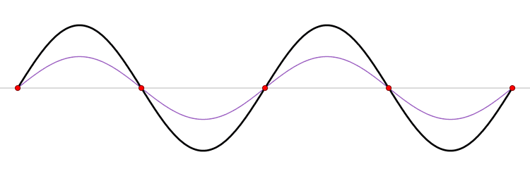
Figure 61: Incident (blue) and reflected (red) voltages and the resulting standing wave (black) produced by a transmission line terminated in a short circuit (point furthest to the right). This animation has been taken from Wikipedia where it is in the public domain.
The red dots conveniently show the nodes, or the locations where the incident and reflected waves are always out of phase. It's clear that the short circuit termination must be a node, because the reflected wave must fully cancel the incident wave. The peaks of the standing wave correspond to the locations where the incident and reflected waves are always exactly in-phase and thus interfere constructively. This animation is designed so that the transmission line length is exactly 2 full wavelengths. However, we could imagine advancing the voltage source by a quarter wavelength so that it was positioned at one of the standing wave peaks (called an antinode). This demonstrates why an impedance mismatch can damage a source: specifically, the voltage amplitude at the source is twice what the source is designed to produce. This won't always damage the source; it depends on the source's output stage.
The reason why a load impedance mismatch causes less energy to reach the load is due to something related to but subtly different from the phenomenon of reflections on a transmission line. It is described by the maximum power transfer theorem, which states that for a finite source impedance, the load impedance which maximizes power delivered to the load is the complex conjugate of the source impedance. It's worth emphasizing this fixed nature of the source impedance, because if you can change the source impedance, you will always increase power delivery to the load by decreasing source impedance. Let's restrict ourselves to strictly real impedance values (that is, resistance values) from now on. A way to think about this theorem conceptually is that even though increasing the load resistance above the source resistance will increase the proportion of the voltage dropped across the load in comparison with the voltage dropped across the source, the total resistance will also increase, decreasing the current through the source and the load. So, increasing the load resistance increases the efficiency, but decreases the total power delivery. The power delivered to the load is
| (8.1.1.2a) | ||||
| (8.1.1.2b) |
From calculus we know that the local maximum or minimum will occur where .
The derivative of the power delivered to the load with respect to the load resistance is
| (8.1.1.3) |
in two cases: as and when
| (8.1.1.4a) | ||||
| (8.1.1.4b) |
The first case corresponds to , which is an asymptotic minimum, and the second case is the maximum we're looking for. The first case and the fact that there are only two solutions here is sufficient to show that the second case is a global maximum. Alternatively, we could compute the second derivative to show the function is concave down at this point.
Finally, it might be tempting to think that this source-load impedance matching requirement would necessitate wasting 50% of the energy at each stage. This is not the case. For instance, power amplifiers are typically designed to present a reactive impedance so that energy is not dissipated inside the amplifier. The tradeoff here is that reactive impedances are inherently frequency-dependent, limiting the bandwidth of these devices. Other devices accept this inefficiency to benefit from the larger bandwidth.
8.1.2. Simulation
When determining the correct width of a microstrip trace to match a desired characteristic impedance, an engineer will often use an approximate equation rather than a full-blown electromagnetic wave simulator. These provide a fairly good approximation for microstrips, which are comparitively simple structures. Although different approximations tend to differ by several ohms from one another, this isn't critical because PCB manufacturers' tolerances tend to be the limiting factor. For instance, even PCB manufacturers that provide controlled-impedance (OSHPark, which this project uses, does not) often only guarantee to be within of the desired impedance. Nonetheless, microstrip impedance is an inexpensive simulation to run and does at least guarantee that any tolerance errors will be centered around the correct value (assuming that any given dimension has an equal probability of deviating in each direction).
The microstrip characteristic impedance over a sweep of trace widths is shown in Figure 62. This is a capability of pyems, which is able to sweep across arbitrary input simulation parameters and perform each simulation in its own process to leverage the multicore nature of most CPUs. The result tells us that we should use a microstrip trace width of .

Figure 62: width is approximately . The calculation was performed for 31 equally-spaced trace width values.
The microstrip transmission line model assumes that there is no coplanar ground plane or ground fill (a ground plane on the same copper layer as the signal trace, shown in Figure 63). This is usually a false assumption because coplanar ground planes plus via fences provide excellent isolation from surrounding traces. The trick is to ensure the coplanar ground plane is far enough away such that most of the field lines are between the adjacent layer ground plane and signal trace instead of the coplanar ground plane and signal trace. Otherwise, you've inadvertently constructed a grounded coplanar waveguide, which will have a somewhat different impedance than the microstrip. We could use a grounded coplanar waveguide instead of the microstrip, but they require narrow gaps between the trace and coplanar ground plane and are therefore more sensitive to manufacturer's tolerances.

Figure 63: Grounded coplanar waveguide cross section.
To determine the necessary separation, we can gradually move the coplanar ground plane further away from the trace and see at what point further movements of the plane no longer have an appreciable effect on characteristic impedance. Equivalently, we can find the minimum gap for which the characteristic impedance is approximately equal to the characteristic impedance we found in Figure 62. I've performed a sweep of the gap between the signal trace and ground plane. The gap is presented as a proportion of the trace width so that we see how many trace widths separation we need. The results are shown in Figure 64.

Figure 64: When the ground gap becomes larger than roughly 100% of the trace width, the coplanar ground plane no longer has an appreciable effect on characteristic impedance.
The simulation results indicate that if the gap width is roughly the same size as the trace width or larger, the coplanar ground plane has little discernable effect on the characteristic impedance of the microstrip.
8.1.2.1. Differential Microstrip
A differential microstrip consists of two identical signal traces separated by a fixed-width gap, as shown in Figure 65. Like a traditional microstrip, there is an uninterrupted ground plane on the adjacent copper layer. The narrow gap between the traces causes some energy to pass between the traces. This is desirable because it means common-mode noise will affect the signal on each trace equally. The differential amplifier that amplifies the differential signal at the input to the next device will have a high common-mode rejection ratio (CMRR) and therefore most of the common-mode noise will be removed.

Figure 65: Differential microstrip cross section.
To keep the coupling factor high, it is important to keep the gap between the traces small. I've used , which is the minimum allowable by OSHPark. I've plotted the differential characteristic impedance across a sweep of trace widths in Figure 66.

Figure 66: width is approximately .
If there were no coupling between the traces, we could simply set the trace width equal to the width for a single microstrip trace with characteristic impedance equal to half the desired differential impedance. However, coupling has the effect of lowering the differential impedance, so the trace width needs to be narrower than the single-ended trace width.
8.2. Horn Antenna
I made 3D-printed horn antennas using the instructions given here. I generated the STL files using OpenSCAD modelled after the Pasternack PE9860-15 antenna. The OpenSCAD code file is included in the main FMCW repository. The simulation structure is shown in Figure 67. A time lapse of the electric field propagation through air due to an excitation of the waveguide in the antenna is shown in Figure 68.
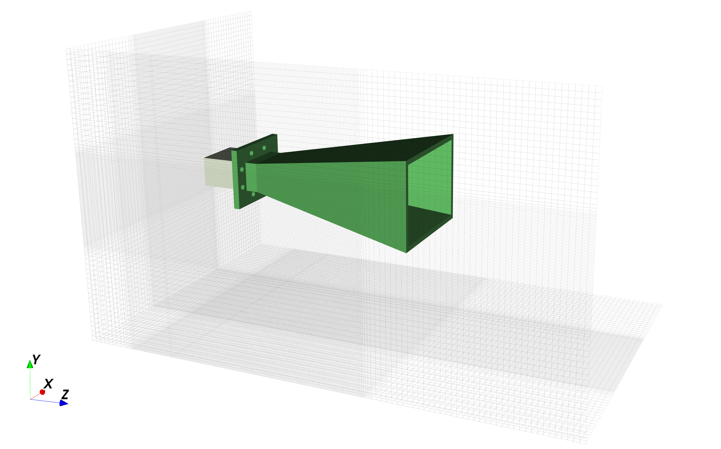
Figure 67: OpenEMS horn antenna structure. The horn structure is created from an STL file, and the waveguide port and mesh are generated by pyems.
Figure 68: The E-field magnitude travelling through a cross-section of the horn.
The simulated return loss is less than throughout the passband, as shown in Figure 69.

Figure 69: Power reflected by the horn antenna in the frequency passband. This is equal to the negative of the return loss.
The plots in Figure 70 show that the radiation pattern has a beamwidth of about (bounded by the angles where the gain drops off by ).

Figure 70: (left) horizontal direction, (right) vertical direction. Both directions have a half-power beamwidth of about .
This is a good directivity value for our target range and demonstrates one of the desirable characteristics of horn antennas, in addition to having a large bandwidth. Having a high directivity value means that a larger percentage of the radiated energy is concentrated in the direction we're pointing the antenna. This is highly desirable for most radars since it increases their range and angular resolution at the cost of needing to pivot the antenna to see in other directions (antenna arrays can do this without pivoting, by injecting deliberate delays to each array element). This might give the impression that directivity is always good but that's not the case. For instance, if a cell phone antenna had high directivity, it would mean that we'd get much better service if we were facing one way than another way, which is obviously not what we want. To that effect, cell phone antennas are designed for as low a directivity as possible. On the other end of the spectrum are dish antennas which have very high directivity and are thus used for very long range applications.
8.3. Directional Coupler
The simplest implementation of a directional coupler (and the implementation used in this design) involves two tightly-spaced microstrip lines. The signal is passed into one end of one of the microstrips, and most of the energy passes through to the other end of the same microstrip. However, some of the energy is coupled into the adjacent microstrip. The amount of coupled energy is inversely related to the separation between the lines, which we can control to achieve a desired energy coupling over a target frequency range.
The maximal coupling between the lines occurs when the line length is a multiple of , where is the signal wavelength in the material (i.e. considering the effective dielectric). The physical reason for this is beyond the scope of this post, but can be found in section 4.2.2 Backward-Wave Directional Couplers in "RF and Microwave Coupled-Line Circuits" by Mongia (2d edition, 1999). This observation also tells us that we can maximize the coupler bandwidth (frequency range in which it provides the desired coupling factor) by setting the coupler length to be one-quarter wavelength for our center frequency of interest (or a positive, non-zero integer multiple of that, but that would waste space). Figure 73 line demonstrates this maximal coupling effect.
A bird's-eye view of the simulated coupler structure is shown in Figure 71.
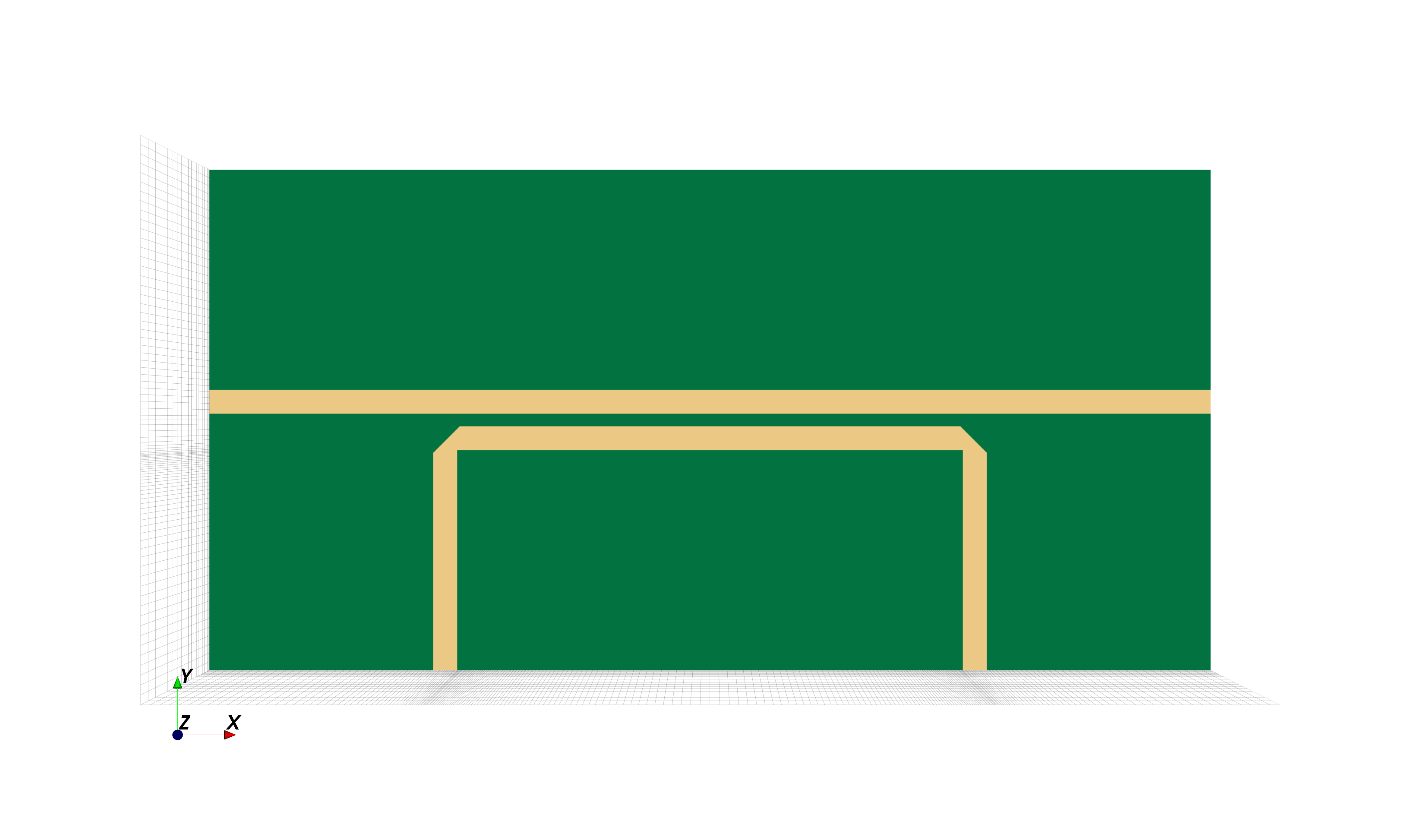
Figure 71: Directional coupler structure in CSXCAD. From upper left proceeding clockwise, the port numbers are 1, 2, 4 and 3.
Animation 72 shows the magnitude of the current density over time for an excitation at port 1.
Figure 72: Animation of the current density magnitude over time for the simulated directional coupler.
The simulation results are shown in Figure 73.

Figure 73: Simulated scattering parameters for the directional coupler, as well as the computed directivity.
and directivity, zoomed into the relevant frequency range, are shown in Figure 74.

Figure 74: and directivity restricted to the signal bandwidth.
The simulation results exhibit the desired coupling factor within the bandwidth of interest. The directivity, on the other hand, is fairly poor. However, as described in the theory section, that does not matter much here. If we had needed a larger bandwidth and/or better directivity, there are many ways to do this.5
8.4. SMA connector
The radar uses a Mueller SMA connector, which is low in cost but still provides good performance in our target frequency range. The simulation structure is shown in Figure 75.
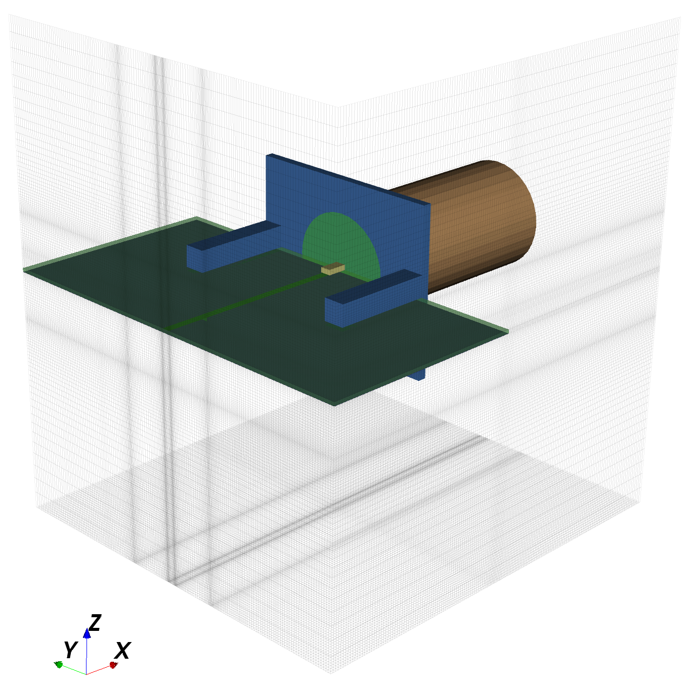
Figure 75: Microstrip - SMA transition simulation structure in CSXCAD.
I've plotted the S-parameter performance of the microstrip to SMA transition from DC to in Figure 76. The return loss is better than throughout the radar frequency range, which equates to a voltage standing wave ratio (VSWR) of about 1.2. This is adequate for our needs. It is worth noting that the performance is somewhat worse than the performance noted in the datasheet, which reports a VSWR of 1.35 at . Our measured VSWR at is 1.55.

Figure 76: Microstrip - SMA transition s-parameters.
8.5. RF Via
A previous iteration of the PCB used an RF via to carry the transmission signal back to the receiver. Although the updated PCB keeps this signal on the top layer, it is worth keeping this section to characterize the behavior of the previous PCB.
Vias change the per-unit-length inductance and capacitance of transmission lines. This is not surprising because the via plating typically has a different surface area than the microstrip trace and the transmission line no longer has a backing copper plane to act as the current return path. The absence of a nearby reference plane decreases the capacitance and thus increases the characteristic impedance of the via. A good way to compensate for this effect is to place vias tied to the reference plane adjacent to the signal via. This construction is shown in Figure 77.
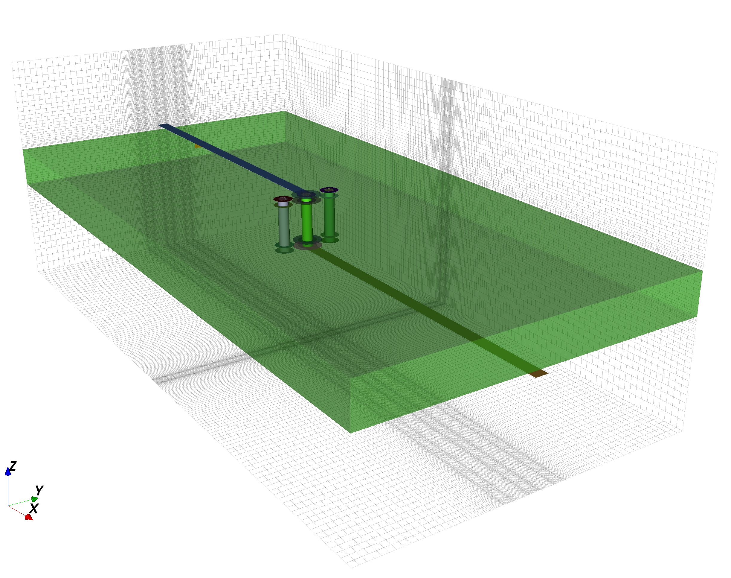
Figure 77: High-frequency via for transitioning signals between the top layer and bottom layer. I've removed the first and last substrate layers as well as the second and third metal layers from the image in order to make the remaining structures easier to see. These omitted structures exist in the actual simulation.
This RF via structure takes inspiration from Henrik's design (see this post). However, I've made an important change: Henrik uses the via to transition the signal between layers 1 and 3, whereas I transition between layers 1 and 4. His construction transitions from a microstrip on the top layer to an asymmetric stripline on the 3rd layer. The main difference between the asymmetric stripline and the microstrip is that the microstrip is bounded by two different dielectrics (the substrate and air), whereas the stripline is bounded by the substrate above and below. In regard to the proximity to the ground reference plane, layers 2 and 3 are much farther apart than layers 3 and 4, so in this way it should behave like a microstrip. If the performance criteria were stringent, it would probably be a good idea to independently characterize the stripline. However, given the comparatively low frequency range of our signal and the manufacturer's tolerance limitations, the performance difference won't matter and so the stripline could be made the same width as the microstrip.
The simulated RF via S-parameters are shown in Figure 78. This performance is more than adequate in our frequency range of interest, and indeed works quite well even up to much higher frequencies.

Figure 78: High-frequency via scattering parameters.
8.6. Series Blocking Capacitor
Several of the radar's transmission lines require a DC blocking capacitor. In an ideal world, adding a series capacitor would simply amount to embedding a large series capacitance into our lumped-element transmission line model. However, this would generate misleading results for several reasons. First and most importantly, capacitors have complicated internal structures that have a significant effect on their frequency response. Additionally, this will ignore mounting considerations: for instance, impedance discontinuities due to the capacitor and its pads having a different width than the microstrip trace. Lastly, if our max frequency is sufficiently high, the capacitor will no longer appear electrically small and cannot be modelled as a lumped-element. This last effect isn't particularly relevant here since the capacitor is still small at .
Although OpenEMS can model lumped elements, doing so would ignore the capacitor's internal structure. Theoretically, if we knew the capacitor's internal structure we could simulate it with OpenEMS, but we'd never want to do this because the simulation would take too long. Fortunately, Murata, which manufactures the high-frequency capacitors I've used in the design, has tested the frequency response of their capacitors with a VNA and made all the information publically-available online. We can use this result directly. This will ignore mounting effects because the simulation data only includes the frequency response of the capacitor.
Typically, a larger capacitor than microstrip width is compensated by removing a small rectangle of ground plane beneath the capacitor. This works because the larger capacitor width increases the lumped-element capacitance and reduces the lumped-element inductance for the length-duration of the capacitor. By removing a section of ground plane beneath the capacitor, we are reducing the capacitance and increasing the inductance. This uses the same principles as a miter, except that with a miter we remove part of the top trace instead of the ground plane. In any event, this compensation technique won't work because this design uses a 0201 capacitor whose width () is less than the microstrip width (). We could compensate for this by bringing the coplanar ground plane closer to the capacitor for the length-duration of the capacitor. However, this is sensitive to the manufacturer's tolerances and it is therefore difficult to achieve consistent results with this strategy. Moreover, the effect should be minimal at . The frequency responses for a 0201 capacitor and 0402 capacitor are plotted in Figure 79.

Figure 79: Murata capacitor parameter. This data has been taken directly from Murata's website.
The performance of the 0201 capacitor is notably better at than the 0402 capacitor. Moreover, the actual frequency response will be slightly worse due to the mounting effects these results ignore. As a result, I've opted to use the 0201 capacitor.
9. Footnotes
Footnotes:
I actually have an upgrade planned for it that should make the angle detection more precise than the original version. I've developed a PCB for it but haven't tested it or written the FPGA code or software to support it yet.
S. He and M. Torkelson. A New Approach to Pipeline FFT Processor. 1996.
C. Cummings. Simulation and Synthesis Techniques for Asynchronous FIFO Design. 2002.
D. Pozar. Microwave Engineering, Fourth Edition. Section 2.1: The Lumped-Element Circuit Model For A Transmission Line.
In particular, RF and Microwave Coupled-Line Circuits (Mongia, 1999) discusses numerous ways to design directional couplers with these goals in mind.